JAJU793 October 2020
- 概要
- リソース
- アプリケーション
- 特長
- 5
- 1System Description
- 2System Overview
-
3Hardware, Software, Testing Requirements, and
Test Results
- 3.1
Hardware Requirements
- 3.1.1 Getting Started
- 3.1.2 Testing and Results
- 3.1
Hardware Requirements
- 4Design and Documentation Support
3.1.2.4 Overcurrent Protection
Overcurrent protection testing primarily consisted of ensuring that the INA302 responded appropriately to increases in current and for the current sense amplifier to turn off LM74810 if an over-current event occurs. As mentioned in section 2.1.1, the INA302 can operate in latch mode or transparent mode. The testing shown in Figure 3-5 and Figure 3-6 was performed in latch mode.
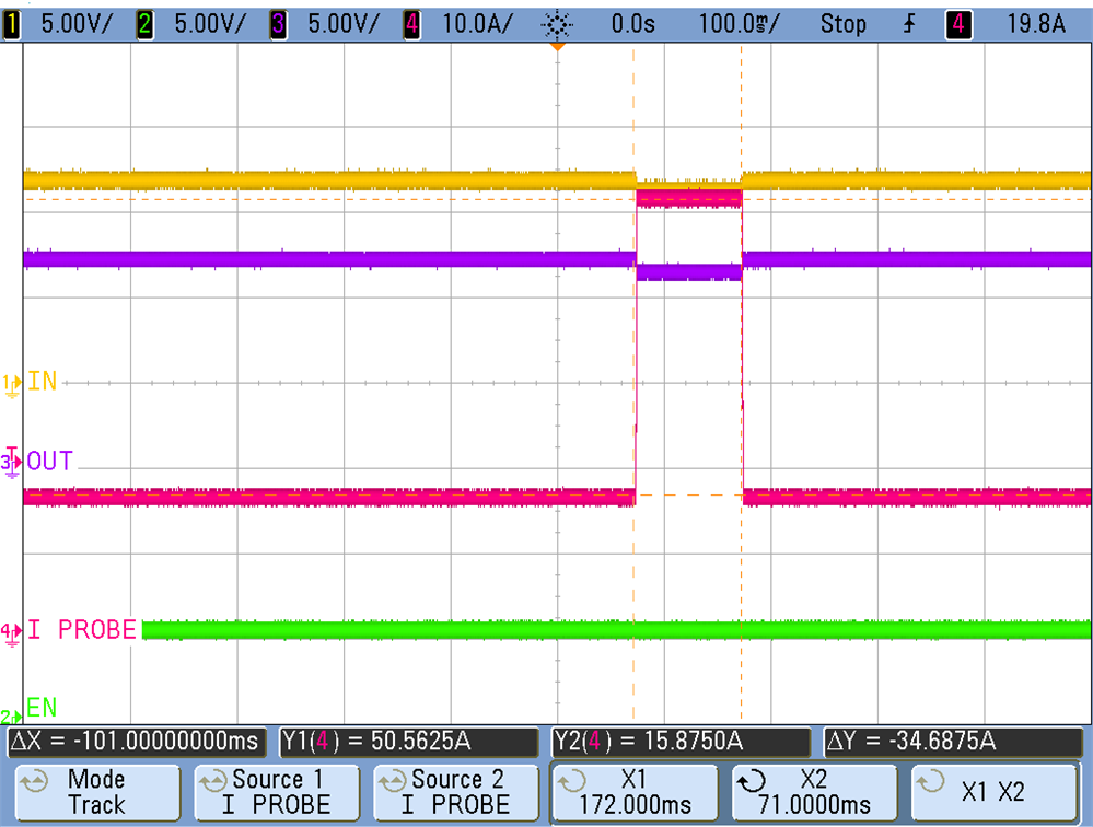
 Figure 3-5 Normal Transient
Current
Figure 3-5 Normal Transient
CurrentAs shown in Figure 3-5, the red trace is the current output which sees an increase in current from 15A to 50A for 100ms. The overcurrent threshold is at 60A and as such the EN pin stays high in normal transient operation.
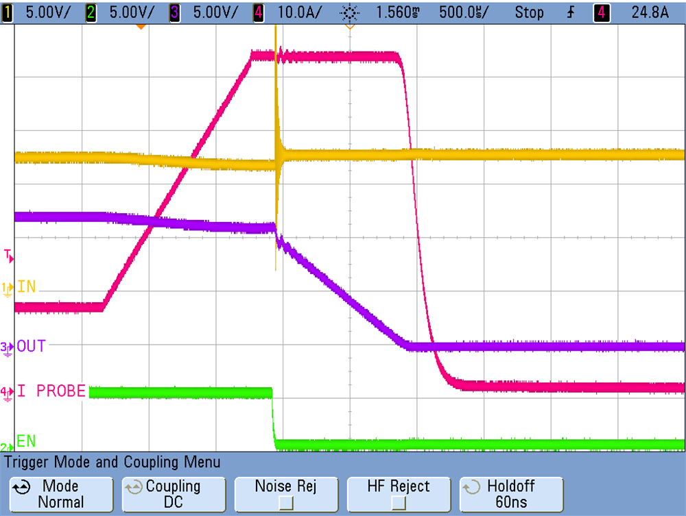
 Figure 3-6 Latch Mode Overcurrent
Protection
Figure 3-6 Latch Mode Overcurrent
ProtectionAs shown in Figure 3-6, the red trace is the current output to the e-load which experiences a 62A transient for 100ms. A 62A transient will trigger the overcurrent protection if the transient last longer than roughly 100µs. The green trace, which is the enable signal, pulls low during the fault conditions and will remain low until the INA302 LATCH pins are toggled to clear the fault. Having the enable signal pulled low, will turn off the MOSFETs, disconnecting the output from the input, resulting in a decrease in output voltage.