JAJU793 October   2020


  1.   概要
  2.   リソース
  3.   アプリケーション
  4.   特長
  5.   5
  6. 1System Description
    1. 1.1 Key System Specifications
  7. 2System Overview
    1. 2.1 Block Diagram
    2. 2.2 Design Considerations
      1. 2.2.1 Ideal Diode Design Overview
      2. 2.2.2 Current Sensing Amplifier Design Overview
      3. 2.2.3 OR Gate Design Overview
      4. 2.2.4 MOSFET Selection
        1. 2.2.4.1 Blocking MOSFET
        2. 2.2.4.2 Hot-Swap MOSFET
      5. 2.2.5 TVS Input Diode Selection
      6. 2.2.6 Inrush Current
    3. 2.3 Highlighted Products
      1. 2.3.1 LM74810-Q1
      2. 2.3.2 INA302-Q1
  8. 3Hardware, Software, Testing Requirements, and Test Results
    1. 3.1 Hardware Requirements
      1. 3.1.1 Getting Started
      2. 3.1.2 Testing and Results
        1. 3.1.2.1 Over-Voltage Protection Cut-Off Mode
        2. 3.1.2.2 Over-Voltage Protection Clamping-Mode
        3. 3.1.2.3 ISO7637-2 Pulse 1
        4. 3.1.2.4 Overcurrent Protection
        5. 3.1.2.5 Load Dump
        6. 3.1.2.6 Cold Crank, Warm Start, and Cold Start
          1. 3.1.2.6.1 Cold Crank
          2. 3.1.2.6.2 Warm Start
          3. 3.1.2.6.3 Cold Start
        7. 3.1.2.7 Standby Current
        8. 3.1.2.8 Currency Sense Accuracy
  9. 4Design and Documentation Support
    1. 4.1 Design Files
      1. 4.1.1 Schematics
      2. 4.1.2 BOM
    2. 4.2 Documentation Support
    3. 4.3 サポート・リソース
    4. 4.4 Trademarks
Warm Start

Warm Start testing is performed to ensure the design functions as appropriate during a warm-start event. Warm Start sees a decrease in battery voltage resulting in the need to ensure the reverse current blocking feature works as intended. As shown in Figure 3-14, the DGATE pulls low when the output voltage is higher than the input voltage to make sure reverse current blocking takes place.
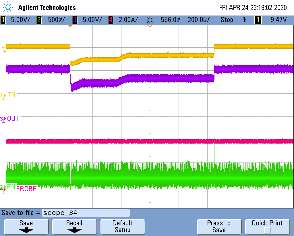
GUID-20200710-SS0I-2X0N-67BP-ZTSKJPCZ7CDM-low.png Figure 3-13 Warm Start/Start Stop Waveform
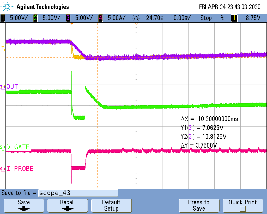
GUID-20200710-SS0I-ZF61-KJ7S-P1PXK9L7DPGP-low.png Figure 3-14 Warm Start Testing