JAJU804D August 2022 – December 2022
- 概要
- リソース
- 特長
- アプリケーション
- 5
- 1System Description
- 2System Overview
- 3Hardware, Software, Testing Requirements, and Test Results
- 4FOTA Example
- 5Design and Documentation Support
- 6Terminology
- 7About the Author
- 8Revision History
2.2.2 Flash Partitioning
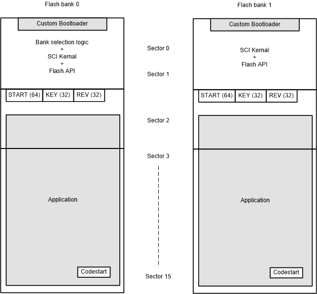
Figure 2-2 shows how the dual-bank Flash is partitioned. Two sectors in each bank are allocated to the custom bootloader, which comprises of Flash bank selection logic, the SCI kernel, and Flash APIs. These do not change during firmware upgrades. Bank 1 does not contain bank selection logic. The rest of the Flash sectors in the bank are allocated to the application. Bank selection logic allows the bootloader to determine which, if any, of the Flash banks are programmed, and which bank contains the more recent application firmware version. By implication, this function is the entry point of the software system. The SCI kernel is a function that implements the transfer of the image from the host, and programming of Flash through Flash programming APIs (either in Flash or in ROM). A few locations in Sector 2 are reserved to store the below information:
- START – Indicates that Flash erase is complete and program/verficication is about to begin.
- Firmware Revision number (REV) – Used by the bank selection logic to determine the newer firmware version between banks 0 and 1.
- KEY – The firmware in a bank is considered valid if this location contains a specific pattern.
 Figure 2-2 Dual Flash Bank
Partitioning