JAJU812 March 2021
- 概要
- リソース
- 特長
- アプリケーション
- 5
- 1System Description
-
2System Overview
- 2.1 Block Diagram
- 2.2
Design Considerations
- 2.2.1 Multichannel SSR with Independent Isolation Between SSR Channels
- 2.2.2 Design Challenge With Single Isolation
- 2.2.3 Multichannel SSR Drive With Single Isolation Multichannel Digital Isolator
- 2.2.4 Need of High-Impedance Voltage Translator
- 2.2.5 Design to Minimize Cross-Coupling and MOSFET Gate Pick up Due to Other SSR Switching
- 2.2.6 Schematic: Design of Gate-Drive Circuit
- 2.2.7 Schematic: Digital Isolator Circuit
- 2.2.8 Schematic: 3.3 V to 10V_ISO, 5V_ISO Power Supply
- 2.3 Highlighted Products
- 3Hardware, Software, Testing Requirements, and Test Results
- 4Design and Documentation Support
- 5About the Author
3.3.5 Alternate SSR Topology for High Voltage
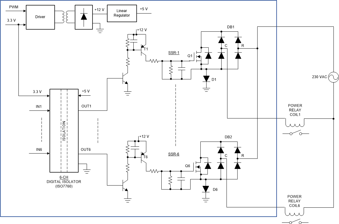
Figure 3-20 shows a cost-effective way of implementing SSRs at higher voltages like 120 VAC or 240 VAC. The SSR circuit normally consists of two back-to-back connected MOSFETs. The high-voltage (240 VAC) SSR needs 600-V MOSFETs and that can be costly. The topology shows a cost-effective SSR where one MOSFET is replaced by four high-voltage slow diodes. The gate drive can be similar to the rest of the part of reference design. Here the PNP transistor T1–T6 needs to be rated for 500 V. The diode D1–D6 has be rated for more than 600 V. The isolation rating of the flyback power supply transformer needs to be appropriately selected.
 Figure 3-20 Circuit Topology for Cost
Reduction at High Voltage