JAJU812 March 2021
- 概要
- リソース
- 特長
- アプリケーション
- 5
- 1System Description
-
2System Overview
- 2.1 Block Diagram
- 2.2
Design Considerations
- 2.2.1 Multichannel SSR with Independent Isolation Between SSR Channels
- 2.2.2 Design Challenge With Single Isolation
- 2.2.3 Multichannel SSR Drive With Single Isolation Multichannel Digital Isolator
- 2.2.4 Need of High-Impedance Voltage Translator
- 2.2.5 Design to Minimize Cross-Coupling and MOSFET Gate Pick up Due to Other SSR Switching
- 2.2.6 Schematic: Design of Gate-Drive Circuit
- 2.2.7 Schematic: Digital Isolator Circuit
- 2.2.8 Schematic: 3.3 V to 10V_ISO, 5V_ISO Power Supply
- 2.3 Highlighted Products
- 3Hardware, Software, Testing Requirements, and Test Results
- 4Design and Documentation Support
- 5About the Author
2.2.3 Multichannel SSR Drive With Single Isolation Multichannel Digital Isolator
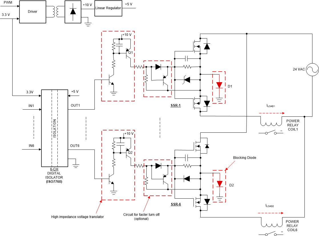
Figure 2-6 shows the topology to drive multiple SSR with single isolating element. In this topology, a 6-channel digital isolator is used to drive six SSR circuits. A single transformer based isolated power supply is used to power the secondary of digital isolator and gate drive. The solution to the problem of unwanted current circulation when one SSR is activated, is to add diodes between common-source of the SSRs to the ground (Blocking diode). Added diodes will prevent load current flow through common ground across multiple SSRs. The diode will block gate discharge of the MOSFET and is solved by adding a PNP transistor circuit and resistor at gate-source of MOSFET. High-impedance voltage translators ensure high-impedance in the MOSFET gate path when digital isolator output is zero, eliminating an otherwise possible small leakage current, that could lead to a false turn on of MOSFET of other SSRs. The functionality of one SSR does not impact the functionality of another SSR.
The turn off of the SSR MOSFET is done through the resistor connected between the gate and source terminals of the MOSFET pair of each SSR. The MOSFET gate will discharge through the turn off resistor when the gate-drive PNP transistor (Q1, Q2) is turned off. The turn off can be made faster by using a PNP transistor across the gate and source of SSR MOSFET pair. The circuit for faster SSR turn off is marked in Figure 2-6 and is optional.
 Figure 2-6 Circuit Topology to Drive
Multiple SSR With Single Isolating Element