JAJU812 March 2021
- 概要
- リソース
- 特長
- アプリケーション
- 5
- 1System Description
-
2System Overview
- 2.1 Block Diagram
- 2.2
Design Considerations
- 2.2.1 Multichannel SSR with Independent Isolation Between SSR Channels
- 2.2.2 Design Challenge With Single Isolation
- 2.2.3 Multichannel SSR Drive With Single Isolation Multichannel Digital Isolator
- 2.2.4 Need of High-Impedance Voltage Translator
- 2.2.5 Design to Minimize Cross-Coupling and MOSFET Gate Pick up Due to Other SSR Switching
- 2.2.6 Schematic: Design of Gate-Drive Circuit
- 2.2.7 Schematic: Digital Isolator Circuit
- 2.2.8 Schematic: 3.3 V to 10V_ISO, 5V_ISO Power Supply
- 2.3 Highlighted Products
- 3Hardware, Software, Testing Requirements, and Test Results
- 4Design and Documentation Support
- 5About the Author
2.2.5 Design to Minimize Cross-Coupling and MOSFET Gate Pick up Due to Other SSR Switching
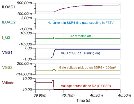
Referring to Figure 2-6, consider the scenario where SSR-6 is kept off and SSR-1 is turned on and off. When SSR-1 is switching, the voltage across the blocking diode D2 changes (the voltage change depends on the instantaneous AC voltage). The voltage change dv/dt across the SSR MOSFETs couples to the blocking diode of SSR6 (which is off) and then through the gate-driver power supply (10 V) low impedance path, couples to the gate-drive transistor circuit (Q2). This can cause momentary base current and resulting collector current in Q2, resulting a gate pick up at the MOSFET gate of SSR6 causing the SSR-6 to conduct. One way to reduce cross coupling is by controlling dv/dt during FET switching, by reducing switching turn on and turn off time by adjusting the gate resistor. The reference design uses decoupling capacitor at the base-emitter of transistor (Q2) to alleviate the unintentional turn on of the gate path transistor Q2, allowing faster MOSFET switching slew rate. The capacitor can be used at the gate to source the of MOSFET to further enhance the noise immunity. shows the simulation results confirming that the gate voltage pick up is negligibly small. The transistor remains off ensuring that there is negligible cross-coupling.
 Figure 2-8 Simulation Results
Illustrating Negligible Cross-Coupling
Figure 2-8 Simulation Results
Illustrating Negligible Cross-CouplingThe performance comparison of the single isolation multichannel SSR topology against other independent isolation SSR topologies and electromechanical relays are listed in Table 2-1.
| Parameter | Electromechanical Relay | SSR: Optical Isolated Drive | SSR: Independent Transformer Isolation | SSR: Single Isolation With Multichannel SSR |
|---|---|---|---|---|
| Cost per relay | Low | High | Medium | Low |
| PCB size per relay | Medium | Low | Medium | Low |
| Life | Low | Medium | High | High |
| Quiescent current per channel | High | Low - Medium | High | Low - Medium |
| Turn on, Turn off time | High | Medium | Medium | Low |