JAJU817 May 2021
- 概要
- リソース
- 特長
- アプリケーション
- 5
- 1System Description
-
2System Overview
- 2.1 Block Diagram
- 2.2 Highlighted Products
- 2.3 Design Considerations
- 3Hardware, Software, Testing Requirements, and Test Results
- 4Design and Documentation Support
- 5About the Author
2.2.2.6 TPS62840
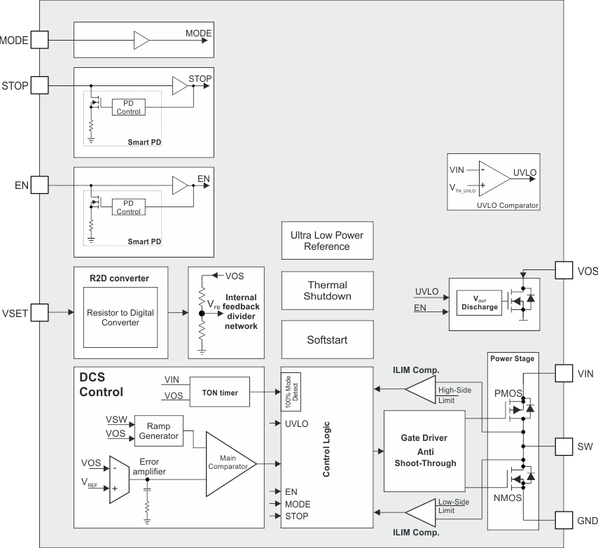
The TPS62840 is a synchronous step-down converter with ultra-low quiescent current consumption. Using TI's DCS-Control™ topology the device extends the high efficiency operation area down to micro amperes of load current during PSM Operation. Depending on the output voltage, the device consumes quiescent current from both the input and output to reduce the overall input current consumption to 60 nA typical. DCS-Control is an advanced regulation topology, which combines the advantages of hysteretic and voltage mode controls. Characteristics of DCS Control are excellent AC load regulation and transient response, low output ripple voltage and a seamless transition between PFM and PWM modes. It includes an AC loop which senses the output voltage (VOS pin) and directly feeds this information into a fast comparator stage. The device operates with a nominal switching frequency of 1.8 MHz. An additional voltage feedback loop is used to achieve accurate DC load regulation. The internally compensated regulation network achieves fast and stable operation with small external components and low ESR capacitors. In PSM, the switching frequency varies linearly with the load current. Since DCS-Control supports both operating modes, the transition from PWM to PFM is seamless with minimum output voltage ripple.
The TPS62840 offers both, excellent DC voltage and superior load transient regulation, combined with low output voltage ripple thereby minimizing interferences with Radio Frequency circuits. Therefore, TPS62840 offers a good alternate to the LDO powering the analog supply rail of the image sensor.
 Figure 2-11 TPS62840 Functional Block
Diagram