JAJU817 May   2021


  1.   概要
  2.   リソース
  3.   特長
  4.   アプリケーション
  5.   5
  6. 1System Description
  7. 2System Overview
    1. 2.1 Block Diagram
    2. 2.2 Highlighted Products
      1. 2.2.1 SimpleLink MCU
        1. 2.2.1.1 CC3235MODS
        2. 2.2.1.2 CC1352R LaunchPad
          1. 2.2.1.2.1 CC1352R
      2. 2.2.2 Power
        1. 2.2.2.1 TPS63802
        2. 2.2.2.2 TPS63900
        3. 2.2.2.3 TPS62825
        4. 2.2.2.4 TPS7A03
        5. 2.2.2.5 TPS7A20
        6. 2.2.2.6 TPS62840
        7. 2.2.2.7 TPS22919
        8. 2.2.2.8 LM66100
      3. 2.2.3 Peripherals
        1. 2.2.3.1 OPT3004
        2. 2.2.3.2 DRV8837C
        3. 2.2.3.3 TPA2011
        4. 2.2.3.4 TLV61048
      4. 2.2.4 OmniVision Video Encoder OA7000
      5. 2.2.5 OmniVision Image Sensor SP2329
      6. 2.2.6 YTOT Lens Module
    3. 2.3 Design Considerations
      1. 2.3.1  Input Power: Battery and USB
      2. 2.3.2  Power Requirements
      3. 2.3.3  Camera Wake-up and Day or Night Sensing
        1. 2.3.3.1 PIR and MSP430 Based Motion Detection Design for Low Cost and High Performance
      4. 2.3.4  Battery Gauging
      5. 2.3.5  IR LED Illumination
      6. 2.3.6  IR Cut Filter
      7. 2.3.7  Audio
      8. 2.3.8  System Operation
      9. 2.3.9  Wi-Fi and Host Subsystem
      10. 2.3.10 Firmware Control
        1. 2.3.10.1 Application Flow
  8. 3Hardware, Software, Testing Requirements, and Test Results
    1. 3.1 Hardware
    2. 3.2 Software
    3. 3.3 Setup
      1. 3.3.1 Configuration Steps for Video over Wi-Fi
      2. 3.3.2 (Optional) Flash OA7000 With Latest Firmware or Stream Video Over USB
      3. 3.3.3 Audio Streaming
      4. 3.3.4 LPSTK-CC1352R Configuration Steps for Camera Module
    4. 3.4 Test Results
      1. 3.4.1 Power Supply Rails and Current Consumption
      2. 3.4.2 Battery Life Calculations
      3. 3.4.3 Video Streaming
      4. 3.4.4 IR LED Drive
  9. 4Design and Documentation Support
    1. 4.1 Design Files
      1. 4.1.1 Schematics
      2. 4.1.2 Bill of Materials
    2. 4.2 Software
    3. 4.3 サポート・リソース
    4. 4.4 References
    5. 4.5 Trademarks
  10. 5About the Author

TPS7A20

Key features of this device include:

  • Low output voltage noise: 7 µVRMS
  • No noise-bypass capacitor required
  • High PSRR: 95 dB at 1 kHz
  • Very low IQ: 6.5 µA
  • Input voltage range: 1.6 V to 6.0 V
  • Output voltage range: 0.8 V to 5.5 V
  • Output voltage tolerance: ±1.5% (max)
  • Very low dropout: 140 mV (max) at 300 mA (VOUT = 3.3 V)
  • Low inrush current
  • Smart enable pulldown
  • Stable with 1 µF minimum ceramic output capacitor
  • Packages: 1 mm × 1 mm X2SON, 0.603 mm × 0.603 mm DSBGA, 2.90 mm × 1.60 mm SOT23-5
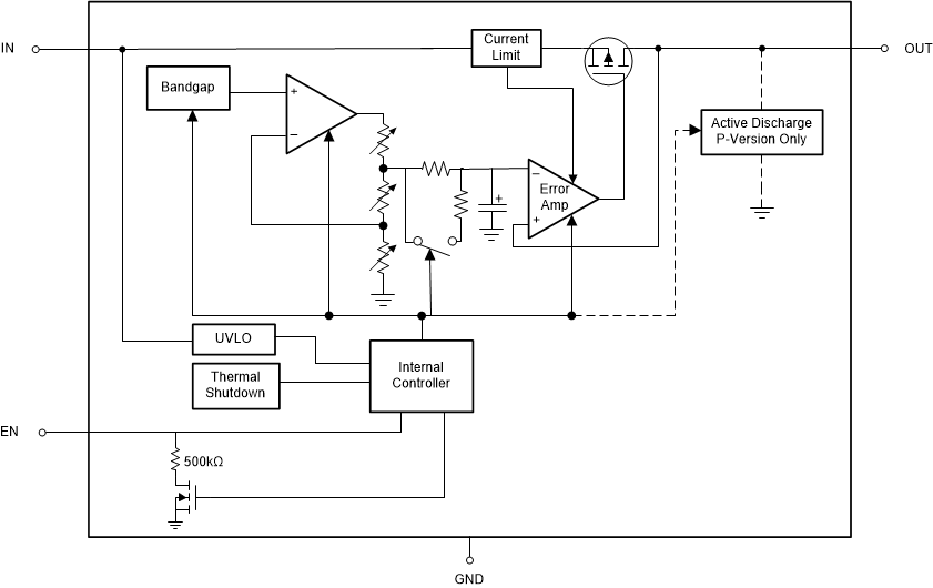
GUID-20200821-CA0I-K5MT-SNV0-CWT9PJJMJCB6-low.gif Figure 2-10 TPS7A20 Functional Block Diagram

The TPS7A20 is an ultra-small, low-dropout (LDO) linear regulator that can source 300 mA of output current. The TPS7A20 is designed to provide low noise, high PSRR, and excellent load and line transient performance that can meet the requirements of RF and other sensitive analog circuits. Using innovative design techniques, the TPS7A20 offers an ultra-low noise performance without the addition of a noise bypass capacitor. The TPS7A20 also provides the advantage of low quiescent current, which can be ideal for battery-powered applications.

Image sensors usually need two power supplies: analog supply and digital supply. The analog supply rail is more sensitive to noise. The TPS7A20 LDO with high PSRR, low noise, and fast transient response is used in this reference design to ensure optimal image qualities. The ability of TPS7A20 to drive high capacitance is also key when powering high-performance image sensors.