JAJU819B April 2021 – June 2021
- 概要
- リソース
- 特長
- アプリケーション
- 5
- 1General Texas Instruments High Voltage Evaluation (TI HV EVM) User Safety Guidelines
- 2System Description
- 3System Overview
-
4Hardware, Software, Testing Requirements, and Test Results
- 4.1 Required Hardware and Software
- 5Design and Documentation Support
- 6Terminology
- 7About the Author
- 8Revision History
- Follow Steps 1 to 4 of the build 1 procedure to enable real-time mode and continuous refresh for the watch views and also for changing the continuous refresh interval for the watch view if needed.
- Run the code by using the <F8> key, or using the Run button on the toolbar.
- Apply an appropriate resistive load to the PSFB system at the DC output. A load that draws around 3A – 6A current at 12 V output is a good starting point.
- Check PSFB_guivLVBus_Set_Volts. PSFB_guivLVBus_Set_Volts should be 2 at the beginning.
- Set PSFB_enable to be 1. This enables PWM output.
- Power the input at J1, J2 with
400V DC (200V and 300V are optional). The output voltage should rise up to
2V.Note:
For user safety, it is recommended to use an isolated DC source to supply 400V DC input to the board.
- Set PSFB_start_flag to 1. The output voltage should now start ramping up to 12 V. Here is the watch view that corresponds to the operation of the system with 12 V at the output with an input voltage of around 400 V and a load of around ~5A (constant current load).
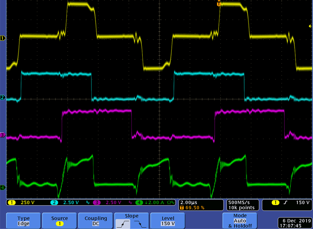
- Gradually increase the load (constant current load) to 25A. The output power will be around 300W. The transformer voltage(CH1), PWM signal(CH2, CH3) and primary current (CH4, primary side of CT) should be similar as Figure 4-12.
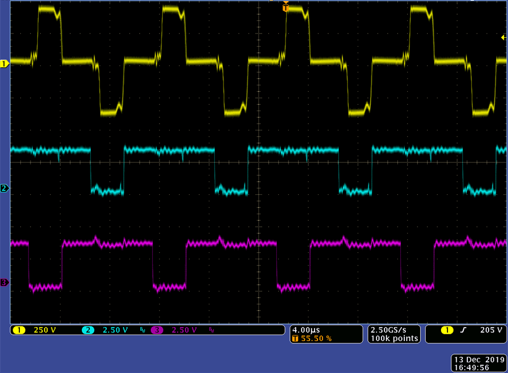
- By default, the synchronous rectifiers are operated in mode 2. You can change their mode of operation by changing PSFB_SR_mode variable to 0, 1 or 2 from the watch view. Observe the change in amount of input current being drawn and change in output voltage with different SR modes. You can also probe the PWM waveforms driving the synchronous rectifier switches. Do not change between different SR modes when operating at very low loads or when the output voltage is very low (less than 6V). In these cases use the default SR mode 2. The SR PWM waveforms(CH2 Ch3) are shown in Figure 4-11
- Now the load transient can be tested. Set the current slew rate to be 0.5A/us (can be tested up to 2.5A). Then set load current to be 12.5A. Now the output power is 150W. More tests can be done between 10% ~ 100% load condition.
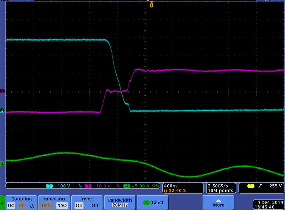
- Probe the MOSFETS Vds and Vgs of active to passive leg and passive to active leg. The low voltage switching is achieved for passive to active leg as Figure 4-10.
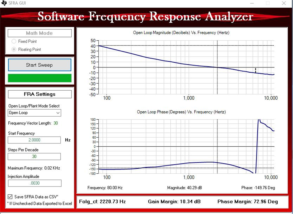
- SFRA is to verify the designed compensator provides enough gain and phase margin by measuring on hardware. To run the SFRA keep the project running, open sfra\gui\SFRA_GUI.exe, SFRA GUI will pop out.
- Select the options for the device on the SFRA GUI. For example, for F28004x select floating point. Click on Setup Connection. On the pop-up window uncheck the boot on connect option, and select an appropriate COM port. Click OK. Return to the SFRA GUI, and click Connect.
- The SFRA GUI will connect to the device. A SFRA sweep can now be started by clicking Start Sweep. Activity can be monitored by seeing the progress bar on the SFRA GUI and also checking the flashing of blue LED on the back on the controlcard that indicates UART activity. When complete, a graph with the open loop plot will appear, as in Figure 4-13. This verifies that the designed compensator is indeed stable.
- Fully halting the MCU when in real-time mode is a two-step process. With the 400 V DC input turned off wait a few seconds. First, halt the processor by using the Halt button on the toolbar, or by using Target > Halt. Then, click the button again to take the MCU out of real-time mode and then reset the MCU.
- Close CCS.
 Figure 4-10 Low Voltage Switching
 Figure 4-11 SR PWM Waveforms
 Figure 4-12 Transformer voltage, PWM and
primary current (primary side of CT) waveforms
 Figure 4-13 Voltage loop SFRA Result