JAJU819B April 2021 – June 2021
- 概要
- リソース
- 特長
- アプリケーション
- 5
- 1General Texas Instruments High Voltage Evaluation (TI HV EVM) User Safety Guidelines
- 2System Description
- 3System Overview
-
4Hardware, Software, Testing Requirements, and Test Results
- 4.1 Required Hardware and Software
- 5Design and Documentation Support
- 6Terminology
- 7About the Author
- 8Revision History
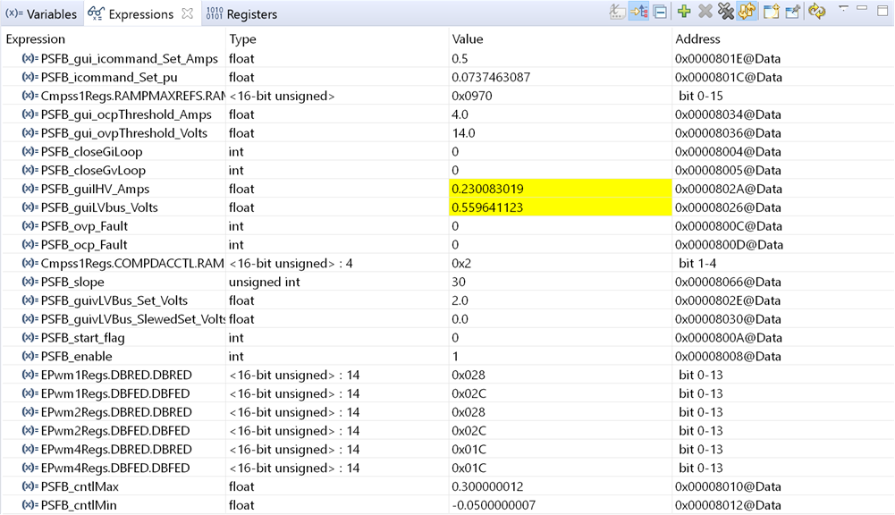
 Figure 4-8 Build 1 Expression Window
- Run the code by using the <F8> key, or using the Run button on the toolbar.
- Apply an appropriate resistive load to the PSFB system at the DC output. A load that draws around 3A – 6A current at 12 V output is a good starting point.
- Set PSFB_gui_icommand_Set_Amps to be 0.5.
- Set PSFB_enable to be 1. This enables PWM output. The expression window is similar to Figure 4-8.
- Power the input at J1, J2 with 390 V DC. The output will be around 1.6 V (5A constant current load).
- Slowly increase PSFB_gui_icommand_Set_Amps to be 2.35 in increments of 0.05. Carefully observe the output voltage(PSFB_guiLVbus_Volts), the voltage should gradually increase to 12 V. This should not be allowed to exceed the capabilities of the board. Different waveforms, like the PWM gate drive signals, input voltage and current and output voltage may also be probed using an oscilloscope. Appropriate safety precautions should be taken and appropriate grounding requirements should be considered while probing these high voltages and high currents for this isolated DC-DC converter.
- The PSFB_slope is set to be 30. User can gradually increase or decrease it for testing.
- Fully halting the MCU when in real-time
mode is a two-step process. With the 400 V DC input turned off wait a few seconds. First,
halt the processor by using the Halt button on the toolbar, or by using Target > Halt.
Then click the
 button again to
take the MCU out of real-time mode and then reset the MCU.