JAJU821 December   2021


  1.   概要
  2.   リソース
  3.   特長
  4.   アプリケーション
  5.   5
  6. 1System Overview
    1. 1.1 Key System Level Specifications
    2. 1.2 System Description
    3. 1.3 Block Diagram
    4. 1.4 Design Considerations
      1. 1.4.1 Frequency Band and Applications
        1. 1.4.1.1 RF Transceiver Synchronization Challenges
        2. 1.4.1.2 JESD204B-Compliant Multichannel Phase Synchronized Clocks Generation
      2. 1.4.2 Clock Jitter and System SNR
      3. 1.4.3 Power-Supply Selection
      4. 1.4.4 Highlighted Products
        1. 1.4.4.1 AFE7950
        2. 1.4.4.2 LMX2820
        3. 1.4.4.3 LMK04832
        4. 1.4.4.4 TPS62913 and TPS62912
        5. 1.4.4.5 LMK1C1104
  7. 2Hardware, Software, Testing Requirements, and Test Results
    1. 2.1 Required Hardware and Software
      1. 2.1.1 Hardware
        1. 2.1.1.1 Clocking Board Setup
        2. 2.1.1.2 FMC-to-FMC Adapter Board Setup
        3. 2.1.1.3 AFE7950EVM Setup
        4. 2.1.1.4 TSW14J56EVM Setup
        5. 2.1.1.5 Hardware Setup of Multiple Transceiver Synchronization
      2. 2.1.2 Software
        1. 2.1.2.1 TIDA-010230 Clocking Board GUI
        2. 2.1.2.2 AFE7950 EVM GUI
        3. 2.1.2.3 High-Speed Data Converter (HSDC) Pro
        4. 2.1.2.4 Programming Steps
        5. 2.1.2.5 Clocking Board Programming Sequence
        6. 2.1.2.6 Latte SW and HSDC Pro Setup
    2. 2.2 Test Setup
    3. 2.3 Test Results
      1. 2.3.1 LMX2820 Phase-Noise Performance
      2. 2.3.2 AFE7950 Transmitter Performance
      3. 2.3.3 AFE7950 Receiver Performance
      4. 2.3.4 Multiple AFE7950s TX and RX Alignment
      5. 2.3.5 Summary and Conclusion
  8. 3Design and Documentation Support
    1. 3.1 Design Files
      1. 3.1.1 Schematics
      2. 3.1.2 BOM
    2. 3.2 Tools and Software
    3. 3.3 Documentation Support
    4. 3.4 サポート・リソース
    5. 3.5 Trademarks
  9. 4About the Author
  10. 5Acknowledgement

Test Setup

Figure 2-7, Figure 2-8, Figure 2-9, and Figure 2-10 show the test setup for LMX2820 phase noise measurement, transmitter performance (SFDR, IMD3) measurement, receiver SNR measurement, and channel-to-channel skew measurement for multiple AFE7950s, respectively.

Use the following steps for each test setup:

  1. Connect a 12-V/3-A power supply to the J23 connector of the clocking board.
  2. Connect two separate 5-V/4-A power supplies to the J35 connector of both AFE7950EVMs.
  3. Connect two separate 5-V/3-A power supplies to the J11 connector of each TSW14J56EVM.
  4. Follow the programming sequence in Section 2.1.2 for each board based on the test setup.
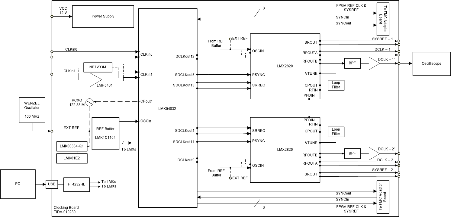
GUID-20211108-SS0I-S5BJ-CPKL-CWQ1DWXKRXQ2-low.gif Figure 2-7 Test Setup for LMX2820 Phase-Noise Measurement
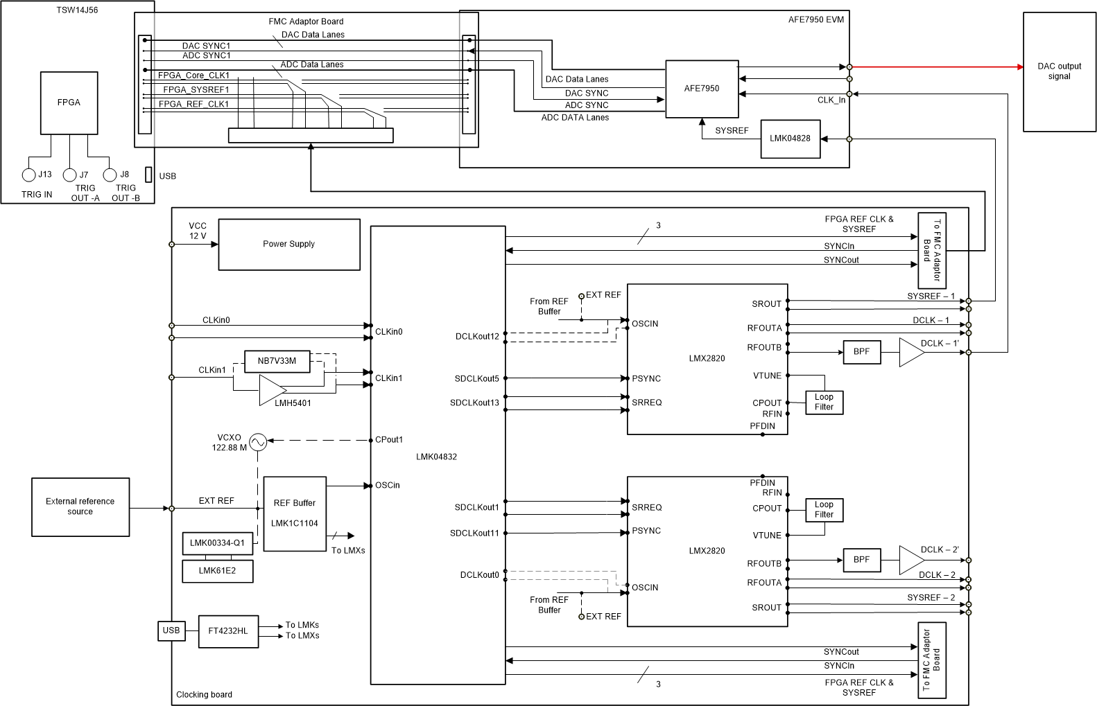
GUID-20211108-SS0I-R5KJ-7R3F-CPK6RKSJZTWK-low.gif Figure 2-8 Test Setup for AFE7950 Transmitter SFDR and IMD3 Measurement
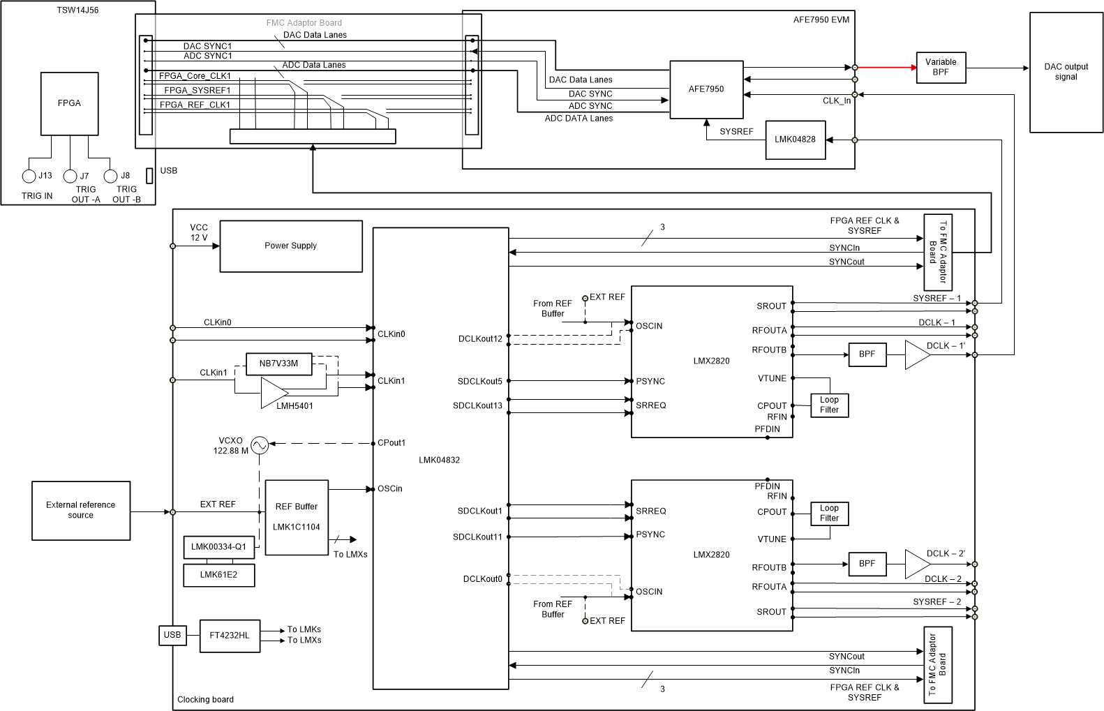
GUID-20211108-SS0I-WXQ8-KNPW-H0LJPWJPDBKP-low.gif Figure 2-9 Test Setup for AFE7950 Receiver SNR Measurement
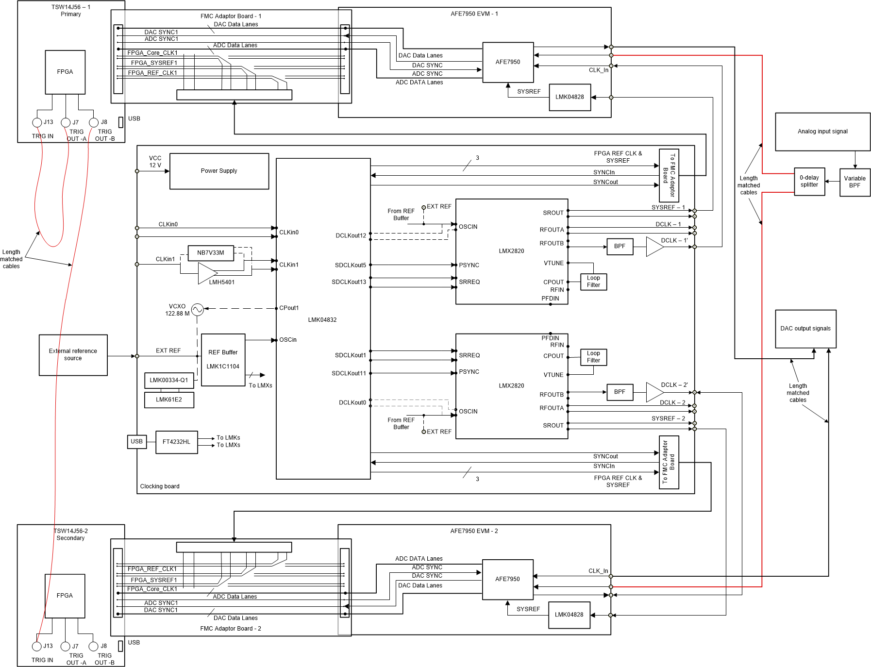
GUID-20211108-SS0I-HFZ8-9LZB-QFVCN1T99SNV-low.gif Figure 2-10 Test Setup for Two AFE7950 Analog Channel-to-Channel Skew Measurement