JAJU855 November 2022 TPS51215A
2.2.4 IMON Output
IMON output is needed by IMVP multiphase VR controller. IMVP controller has related pins for the input and they should be connected with the IMON output from VCCIN_AUX solution.
Currently, there are two major types of IMON output signal, which is determined by the used IMVP VR controller:
- The first type of IMON output is inductor DCR current sensing signal. For this type of IMON, the IMVP VR controller has two pins for differential IMON input. The solution proposed in this reference design is compatible with this type of IMVP VR controller. The differential voltage signals on Cfilter1 in Figure 2-1 are the IMON output and could be directly connected with VR controller.
- The second type of IMON output is a single-ended voltage proportional to inductor average current and referenced to ground. The solution proposed in this reference design is not compatible with this type of IMVP controller.
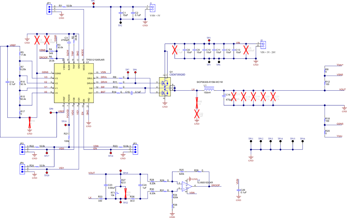
The schematic design is shown as Figure 2-2.
 Figure 2-2 TPS51215A Power Solution with
Load Line Feature Schematic
Figure 2-2 TPS51215A Power Solution with
Load Line Feature SchematicFigure 2-2 is the major page of schematic in this reference design, which only includes the circuits around voltage regulator. The symbol for test tool interposer and the output capacitors placed at loading side (interposer side) are not shown here.
The complete schematics of the reference design are at TIDA-050057.
The principle for implementation will be introduced in Section 2.4.