JAJU855 November   2022 TPS51215A


  1.   概要
  2.   リソース
  3.   特長
  4.   アプリケーション
  5.   5
  6. 1System Description
  7. 2System Overview
    1. 2.1 Block Diagram
    2. 2.2 Design Considerations
      1. 2.2.1 DCR current sense
      2. 2.2.2 Subtract and Amplify
      3. 2.2.3 Active Voltage Scale
      4. 2.2.4 IMON Output
    3. 2.3 Highlighted Products
    4. 2.4 System Design Theory
      1. 2.4.1 DCR Current Sense
      2. 2.4.2 Subtract and Amplify
      3. 2.4.3 Active Voltage Scale
      4. 2.4.4 IMON Output
  8. 3Hardware, Software, Testing Requirements, and Test Results
    1. 3.1 Hardware Requirements
    2. 3.2 Test Setup
    3. 3.3 Test Results
      1. 3.3.1 Start-up
      2. 3.3.2 VID Change
      3. 3.3.3 Load Transient
      4. 3.3.4 Load-Line Test
  9. 4Design and Documentation Support
    1. 4.1 Design Files
      1. 4.1.1 Schematics
      2. 4.1.2 BOM
      3. 4.1.3 PCB Layout Recommendations
      4. 4.1.4 Altium Project
      5. 4.1.5 Gerber Files
      6. 4.1.6 Assembly Drawings
    2. 4.2 Documentation Support
    3. 4.3 サポート・リソース
    4. 4.4 Trademarks
  10. 5About the Authors

Test Setup

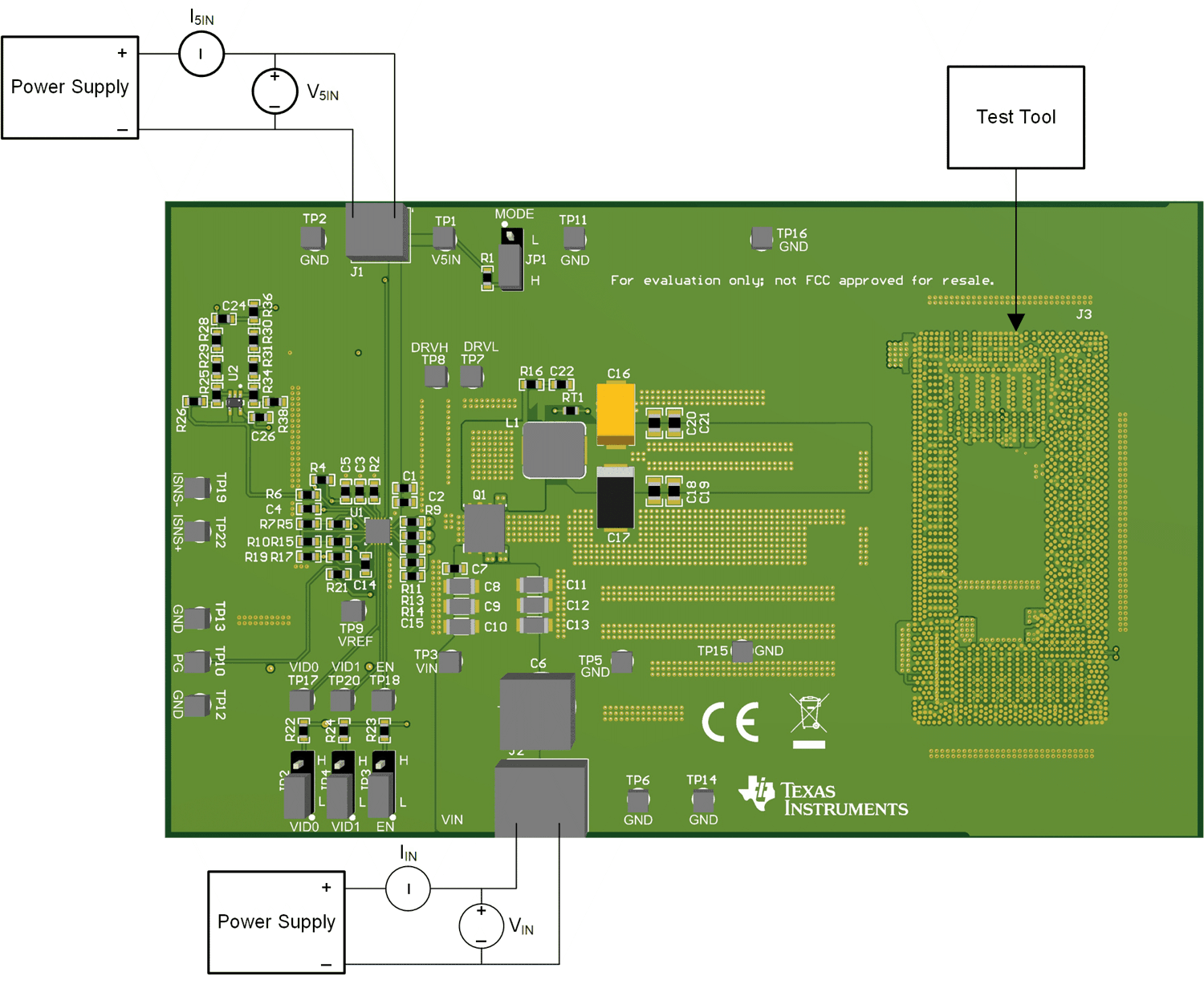
Figure 3-1 shows the set up used to test the TIDA-050057. Test tool refers to Intel® VR Test Tool. The following start-up procedure is shown below.

  1. Jump the JP2 and JP4 according to required VID output voltage or connect external drive signals to the TP17 and TP20.
  2. Apply proper DC voltage to J1 and J2. Apply J2 with external power source first and then apply J1 5 V with another power source.
  3. Jump the JP3 to high to enable the device or connect external drive signals to TP18.
  4. Check the output.
GUID-20220503-SS0I-C3SD-WLBW-9CDDZV8WGQZ9-low.png Figure 3-1 Test Setup