JAJU858 December 2022
- 概要
- リソース
- 特長
- アプリケーション
- 5
- 1System Description
-
2System Overview
- 2.1 Block Diagram
- 2.2
Design Considerations
- 2.2.1
Isolated AC/DC Power Supply Design
- 2.2.1.1 Input Bulk Capacitance and Minimum Bulk Voltage
- 2.2.1.2 Transformer Turns-Ratio, Primary Inductance, and Primary Peak Current
- 2.2.1.3 Transformer Parameter Calculations: Primary and Secondary RMS Currents
- 2.2.1.4 Main Switching Power MOSFET Selection
- 2.2.1.5 Rectifying Diode Selection
- 2.2.1.6 Output Capacitor Selection
- 2.2.1.7 Capacitance on VDD Pin
- 2.2.1.8 Open-loop Voltage Regulation Versus Pin Resistor Divider, Line Compensation Resistor
- 2.2.1.9 Feedback Elements
- 2.2.1.10 Backup Power Supply
- 2.2.1.11 Supercapacitor Selection
- 2.2.1.12 Supercapacitor Charger Design
- 2.2.2 Control Pilot Signal Interface
- 2.2.3 Relay Drive and Weld Detect
- 2.2.4 Residual Current Detection
- 2.2.1
Isolated AC/DC Power Supply Design
- 2.3 Highlighted Products
- 3Hardware, Testing Requirements, and Test Results
- 4Design and Documentation Support
- 5About the Author
2.2.4.8 Full-Wave Rectifier
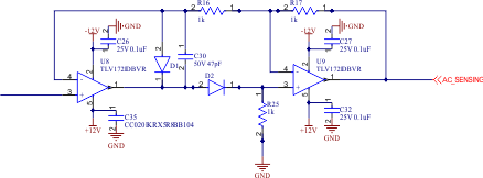
The full-wave rectifier only flips negative voltage to positive. The full-wave rectifier allows the same trip threshold for negative and positive fault current. The other reason for using the full-wave rectifier is to convert the negative polarity of the signal to positive voltage within the input range of the ADC of the MCU and prevent Electrical Overstress (EOS).
 Figure 2-14 Full-Wave Rectifier Schematic
This precision full-wave rectifier can turn alternating current (AC) signals to single polarity signals. The op amps, U8 and U9, buffer the input signal and compensate for the voltage drops across D1 and D2 allowing for small signal inputs. The circuit is used in this application to quantify the absolute value of input signals which have both positive and negative polarities.
This topology was chosen over other full-wave rectifier topologies for the simplicity while achieving the desired performance. U1A and U1B control the biasing of D1 and D2 to change the signal path based on the polarity of the input signal achieving the full-wave rectification. The input impedance of the circuit is set by the termination resistor R4 and can be set to match the source impedance or as high as the input impedance of the U1A amplifier.
Figure 2-16 and Equation 62 show the circuit schematic and transfer function for positive input signals. Positive input signals reverse-bias D1 and forward-bias D2 making the components act like an open circuit and short circuit, respectively. In this configuration, the U1A amplifier drives the non-inverting input of U1B such that the voltage at the inverting input of U1A is equal to VIN. Because current does not flow into the high-impedance inverting input of U1A, there is no current through R1 or R2 and U1B acts as a buffer. U1A must therefore also act as a buffer and VOUT is simply equal to VIN.
Figure 2-17 and Equation 63 show the circuit and transfer function for negative inputs. Negative input signals forward bias D1 and reverse bias D2. Therefore, U1A drives U1B like a standard inverting amplifier while R3 biases the non-inverting node of U1B to GND. In this configuration, the output is now positive for negative input signals achieving the full-wave rectification.