JAJU858 December 2022
- 概要
- リソース
- 特長
- アプリケーション
- 5
- 1System Description
-
2System Overview
- 2.1 Block Diagram
- 2.2
Design Considerations
- 2.2.1
Isolated AC/DC Power Supply Design
- 2.2.1.1 Input Bulk Capacitance and Minimum Bulk Voltage
- 2.2.1.2 Transformer Turns-Ratio, Primary Inductance, and Primary Peak Current
- 2.2.1.3 Transformer Parameter Calculations: Primary and Secondary RMS Currents
- 2.2.1.4 Main Switching Power MOSFET Selection
- 2.2.1.5 Rectifying Diode Selection
- 2.2.1.6 Output Capacitor Selection
- 2.2.1.7 Capacitance on VDD Pin
- 2.2.1.8 Open-loop Voltage Regulation Versus Pin Resistor Divider, Line Compensation Resistor
- 2.2.1.9 Feedback Elements
- 2.2.1.10 Backup Power Supply
- 2.2.1.11 Supercapacitor Selection
- 2.2.1.12 Supercapacitor Charger Design
- 2.2.2 Control Pilot Signal Interface
- 2.2.3 Relay Drive and Weld Detect
- 2.2.4 Residual Current Detection
- 2.2.1
Isolated AC/DC Power Supply Design
- 2.3 Highlighted Products
- 3Hardware, Testing Requirements, and Test Results
- 4Design and Documentation Support
- 5About the Author
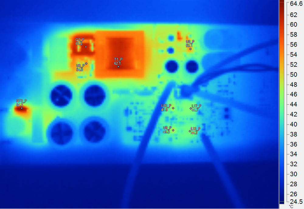
3.3.1.5 Thermal Performance
 Figure 3-31 Top View of AC/DC Stage at
120-V AC, 60-Hz AC Input
Figure 3-31 Top View of AC/DC Stage at
120-V AC, 60-Hz AC InputTable 3-6 Main Image Markers (Top
Side)
|
NAME |
TEMPERATURE |
EMISSIVITY |
BACKGROUND |
|---|---|---|---|
|
RT3_P |
64.3°C |
0.96 |
25.5°C |
|
Q2_P |
61.3°C |
0.96 |
25.5°C |
|
T1_P |
62.1°C |
0.96 |
25.5°C |
|
U8_P |
53.1°C |
0.96 |
25.5°C |
|
U13_P |
47.9°C |
0.96 |
25.5°C |
|
U9_P |
49.3°C |
0.96 |
25.5°C |
|
L17_P |
44.7°C |
0.96 |
25.5°C |
|
L13_P |
44.2°C |
0.96 |
25.5°C |
|
U3_P |
54.0°C |
0.96 |
25.5°C |
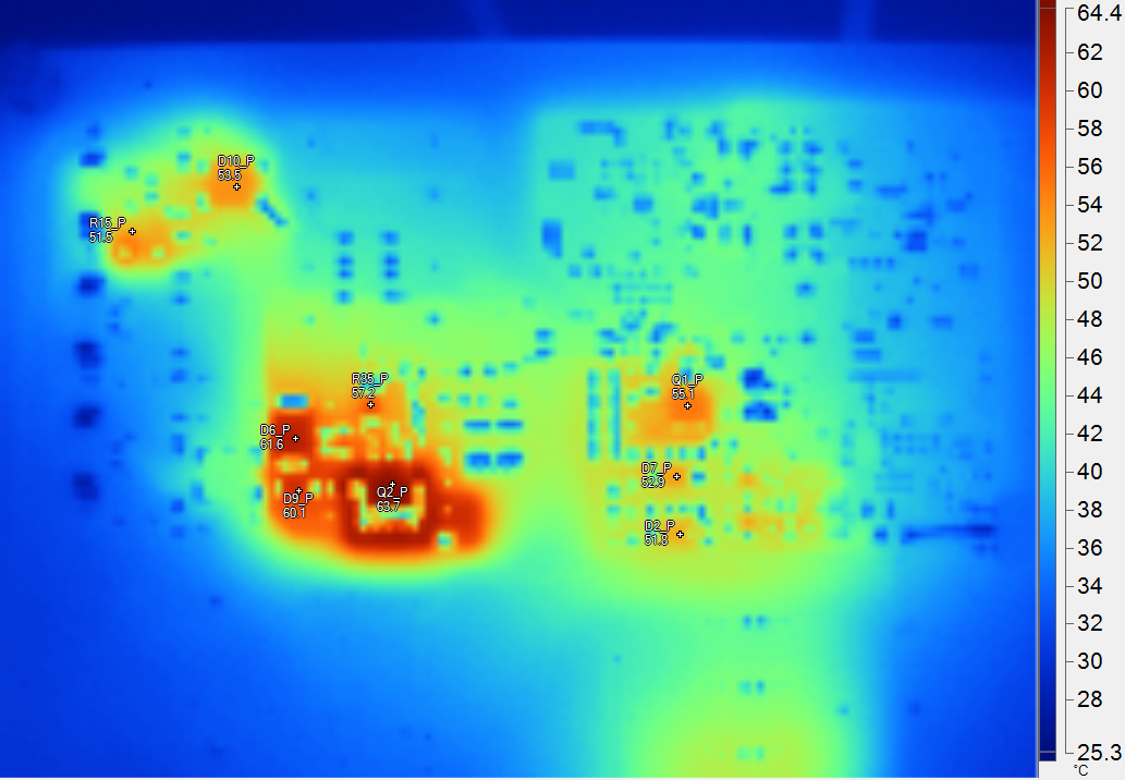
 Figure 3-32 Bottom View of AC/DC Stage at
120-V AC, 60-Hz AC Input
Figure 3-32 Bottom View of AC/DC Stage at
120-V AC, 60-Hz AC InputTable 3-7 Main Image Markers (Bottom
Side)
|
NAME |
TEMPERATURE |
EMISSIVITY |
BACKGROUND |
|---|---|---|---|
|
D10_P |
53.5°C |
0.96 |
25.5°C |
|
R15_P |
51.5°C |
0.96 |
25.5°C |
|
D6_P |
61.6°C |
0.96 |
25.5°C |
|
D9_P |
60.1°C |
0.96 |
25.5°C |
|
Q2_P |
63.7°C |
0.96 |
25.5°C |
|
R35_P |
57.2°C |
0.96 |
25.5°C |
|
Q1_P |
55.1°C |
0.96 |
25.5°C |
|
D7_P |
52.9°C |
0.96 |
25.5°C |
|
D2_P |
51.8°C |
0.96 |
25.5°C |