JAJU873 August 2020
- 概要
- リソース
- 特長
- アプリケーション
- 5
- 1 System Description
- 2System Overview
- 3Hardware, Software, Testing Requirements, and Test Results
- 4Design and Documentation Support
- 5About the Author
2.2.1.1 DRV8323RS BLDC Motor Driver Design Calculations
External MOSFET Support
The DRV832x MOSFET support is based on the capacity of the charge pump and PWM switching frequency of the output. For a quick calculation of MOSFET driving capacity, use the following equations for three phase BLDC motor applications.
Trapezoidal 120° Commutation:
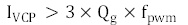
Sinusoidal 180° Commutation and FOC:
where
- ƒpwm is the maximum desired PWM switching frequency
- IVCP is the charge pump capacity, which depends on the VM pin voltage
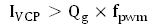
- The multiplier based on the commutation control method, may vary based on implementation
- Qg is the total gate charge
The DRV8323RS device is capable of supporting PWM frequencies up to 200 kHz and the selected CSD88584Q5DC power block is capable of 50 kHz. However, the actual PWM frequency will be limited by the charge pump specification. For a VM supply voltage ≥ 13 V, the charge pump is rated for 25 mA and the Vcp operating voltage is 11 V relative to VM. From the CSD88584Q5DC data sheet, the typical Qg is rated at 137 nC (178 nC max).
The maximum 24-V application PWM frequency operating FOC is:
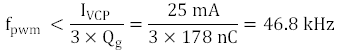
In this design, the PWM frequency was set to 45 kHz.
Power Dissipation Calculations
The maximum input supply of 28 V and Iload of 10 A were used for the following calculations. These calculations are applicable for sinusoidal PWM (SPWM) and FOC motor controls. Note, for sinusoidal and FOC, each FET has 180o of conduction. The CSD88584q5dc and DRV8323RS data sheets were referenced for the electrical specifications. Each loss type is split evenly between the high and low FETs.
Half-bridge FET Losses
The max conduction loss for the half-bridge is:

The 1.5 correction factor accounts for junction temperature effect on the FET resistance. That is, a 50% increase in resistance due to temperature. This is a rule-of-thumb for moderate junction temperature (50-100 oC). If the FET junction operates at 125 oC, this factor must be adjusted accordingly (e.g. 1.8 instead).
The DRV8323 can source and sink up to 1A and 2A, respectively. The rise and fall switching times are:
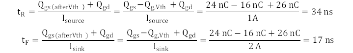
where tR and tF are the switching times (including the rise and fall times) corresponding to the rise and fall transitions.
The max switching loss for the half-bridge is (assume negligible soft switching losses):

The dead time loss is:
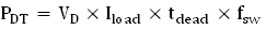

The DRV8323RS’s dead time is programmable with 50-ns, 100-ns, 200-ns, and 400-ns options. The default setting is 100 ns. There are two instances of dead time per a switching cycle.
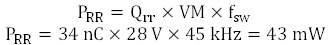
The reverse recovery charge loss is:
The gate drive voltage is 11 V (typical) for VM >13 V and the Qg (Vgs =10 V) is 178 nC from the data sheet.
Assume half of the gate charge loss is on the FET side and half on the driver IC side. The half-bridge gate charge loss is:
The total half-bridge loss is:

DRV8323RS Driver Losses
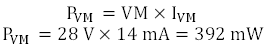
The operating supply current loss is:
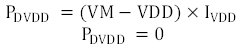
For high-side (HS) driver supply loss, assume a 50% charge pump efficiency:
For low-side (LS) driver supply loss:
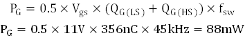
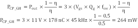
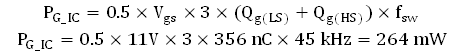
For gate drive loss inside driver IC, again assume half is on the driver side. Note, the driver drives three half-bridges:
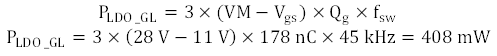
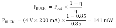
For the DRV8323RS integrated buck (LMR16006X), assume a maximum load of 200 mA and an 85% efficiency:
The total driver IC loss is:

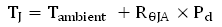
Junction Temperature Estimation
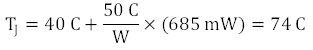
For CSD88584q5dc power block, assume a RθJA = 50 °C/W (1 in2 of 2-oz Cu) based on the data sheet:
For DRV8323RS (RGZ package) driver, assume a RθJA = 26.6 °C/W based on the data sheet:
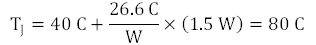
These temperature estimates are well below the max ratings, which allows for an adequate operating margin.
IDRIVE Configuration
The strength of the gate drive current, IDRIVE, is selected based on the gate-to-drain charge of the external MOSFETs and the target rise and fall times at the outputs. If IDRIVE is selected to be too low for a given MOSFET, then the MOSFET may not turn on completely within the tDRIVE time and a gate drive fault may be asserted. In this design, the default IDRIVE was set to 1A/2A (default). However, for most applications, a lower drive current is recommended to reduce EMI.
VDS Overcurrent Monitor Configuration
The VDS monitors are configured based on the worst-case motor current and the RDS(on) of the external MOSFETs. Using a 1.8 temperature factor for 0.95 mΩ, the max RDS(on) is 1.7 mΩ. The target OCP threshold is 30 A so VDS_OCP must be:
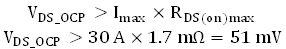
The VDS_OCP threshold was set to 60 mV (closest available) and the OCP deglitch time was set to 4 µs (default).
Unidirectional Current Sense Operation
The sense amplifier gain and sense resistor values are selected based on the target current range, VREF, power rating of the sense resistor, and operating temperature range. In unidirectional operation of the sense amplifier, use the following equation to calculate the approximate value of the dynamic range at the output:
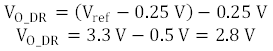
Using the default gain of 20 V/V and the maximum input current of 12 A (10 A plus a 20% margin):
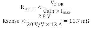
10 mΩ was selected for Rsense. The minimum power rating for Rsense must be:

In this design, a 10-mΩ, 3-W Rsense was used for each of the three channels. In addition, 1.3-kHz RC low pass filters were used for these sensing channels to limit noise.
The full scale ADC current is (ignore the headroom limitation):
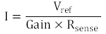
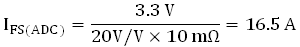
This value is defined as USER_ADC_FULL_SCALE_CURRENT_A in the user.h file.
Buck Regulator Configuration
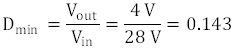
The LMR16006 buck is capable of supplying up to 600 mA. The switching frequency is fixed at 700 kHz (typical). In this design, the buck was configured for a 4-V output. The expected application load is 200 mA. This 4-V rail is the primary supply for the digital loads. The basic inductor calculations are shown below. For more information, please reference the LMR16006 data sheet design example.
The first step to calculate the peak inductor/switch current is to determine the duty cycle, D, for the maximum input voltage. The maximum input voltage is used because this leads to the maximum switch current:
The parameters for selecting the inductor are the inductance and saturation current. The inductance is based on the desired peak-to-peak ripple current and is normally chosen to be in the range of 20 to 40 % of the maximum output current. Note that when selecting the ripple current for applications with much smaller maximum load (0.2 A) than the maximum available from the device (0.6 A), the maximum device current should be used:
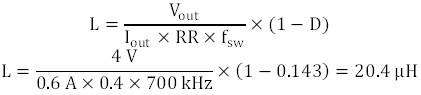
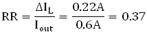
RR of 0.4 was selected.
For this design, 22 μH was selected.
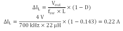
The actual worst-case ripple current is:
The actual ripple ratio is:
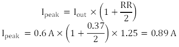
The peak inductor/switch/diode current and the minimum saturation current rating of the inductor plus a 25% margin are calculated as follows:
The LMR16006 has a current limit at 1.7 A (max). Using a saturation rating near 1.7 A will enable the LMR16006 to current limit without saturating the inductor. This is preferable to the LMR16006 going into thermal shutdown mode and the possibility of damaging the inductor if the output is shorted to ground or other long-term overload.
In this design, the selected inductor (74438356220) has saturation ratings of 1.85 A (ΔL=-20%). Based on the data sheet, this inductor RMS rating is well suited to handle 1.7 A with a 40 oC rise.
For the RMS current calculations, the 0.2 A max application current is used instead of the device maximum:
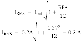
Note, IRMS is approximately Iout given a small RR value.
Inductor wire loss is calculated as follows:

Temperature monitor and over temperature protection
The design is equipped with three TMP1075 digital temperature sensors designed to monitor and protect the power blocks. Three TMP1075 ALERT outputs (active low) and the DRV8323RS Enable control signal are connected to a quad-input AND gate. The DRV8323RS will be disabled if one of the inputs is logic LOW.