JAJU873 August 2020
- 概要
- リソース
- 特長
- アプリケーション
- 5
- 1 System Description
- 2System Overview
- 3Hardware, Software, Testing Requirements, and Test Results
- 4Design and Documentation Support
- 5About the Author
2.2.3.3 LMR33630 Buck Design Calculations
Based on the key system specification, the maximum solenoid load is 1.7 A. The boost-buck DC-DC power stage, consisting of LM5211 and LMR33630, is designed to support 2 A of continuous load. Note, WEBENCH® Power Designer was used to help design the power stage. The key design calculations for the LMR3360 Buck Stage are shown below. For more details on design considerations, please refer to the device data sheet.
| PARAMETER | SPECIFICATION | COMMENTS |
|---|---|---|
| Input Voltage | 14-28 V | From boost stage |
| Input Power | 26.7 W | Max, η = 90% |
| Output Voltage | 12 V | For solenoid drive |
| Output Power | 24 W | Max |
| Max Load Current | 2 A | Vout = 12 V (24 W) |
The choice of switching frequency is a compromise between conversion efficiency and overall solution size. For this design, 400 kHz was chosen (i.e. LMR33630A variant) as a compromise between efficiency and overall solution size.
Setting the Output Voltage
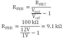
The output voltage of the LMR33630 is externally adjustable using a resistor divider network. The target output is 12 V. Start with the recommended 100 kΩ value. The RFBB is:

9.1 kΩ was selected.
Inductor Selection
The first step to calculate the peak inductor/switch current is to determine the duty cycle, D, for the maximum input voltage. The maximum input voltage is used because this leads to the maximum switch current:

The parameters for selecting the inductor are the inductance and saturation current. The inductance is based on the desired peak-to-peak ripple current and is normally chosen to be in the range of 20-40 % of the maximum output current. Note that when selecting the ripple current for applications with much smaller maximum load (2 A) than the maximum available from the device (3 A), the maximum device current should be used.

The maximum inductance is limited by the minimum current ripple required for the current mode control to perform correctly. As a rule-of thumb, the minimum inductor ripple current must be no less than about 10% of the device maximum rated current under nominal conditions:

From the data sheet, the minimum inductance is given by:

RR of 0.3 was selected for the following inductance calculation:

For this design 33 μH was selected. This value is inside the recommended inductance range. Alternatively, a smaller inductance 22 μH (SPM7054VT-220M-D) could be used since the saturation current rating would be higher.
The actual worst-case ripple current is:

The actual ripple ratio is:

The peak inductor/switch/diode current and the minimum saturation current rating of the inductor plus a 25% margin are calculated as follows:

However, the LM33630 has specific inductor saturation requirement for its normal operation due to internal current limits. Ideally, the saturation current rating of the inductor must be at least as large as the high-side switch current limit, ISC. The ISC is 4.5 A typical and 5 A max.
In any case, the inductor saturation current must not be less than the device low-side current limit, ILIMIT. The ILIMIT is 3.5 A typical and 4.1 A max.
In this design, the selected inductor (SPM7054VT-330M-D) has saturation ratings of 3.6 A (ΔL=-20%) and 4.9 A ΔL=-30%). Based on the data sheet, this inductor RMS rating is well suited to handle 3.4 A with a 40 oC rise.
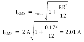
For the RMS current calculations, the 2 A max application current is used instead of the device maximum:

Note, IRMS is approximately Iout given a small RR value.
Inductor wire loss is calculated as follows:

Output Capacitor Selection
The value of the output capacitor and the ESR of the capacitor determine the output voltage ripple and load transient performance. The output capacitor bank is usually limited by the load transient requirements, rather than the output voltage ripple. The following equations can be used to estimate a lower bound on the total output capacitance and an upper bound on the ESR, which is required to meet a specified load transient. Assume a 2 A transient step with 5% voltage drop (600 mV), using the worst-case input:


In this design, three 22-μF and one 1-μF were used, which accounts for tolerance and voltage derating. These ceramic caps are rated for 25 V, so the de-rated output capacitance is 32 μF. Ceramic capacitors can easily meet the minimum ESR requirements. Assume an effective ESR of 50 mΩ for the ripple voltage calculations.
The peak-to-peak output voltage ripple is:

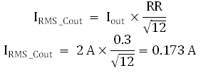
The output cap RMS current is:

Input Capacitor Selection
The ceramic input capacitors provide a low impedance source to the regulator in addition to supplying the ripple current and isolating switching noise from other circuits. A minimum of 10 µF of ceramic capacitance is required on the input of the LMR33630. This must be rated for at least the maximum input voltage (28 V). For this design, 10-µF and 220-nF ceramic caps were selected. Both capacitors are rated at 50 V, which accounts for voltage-derating.
The input cap RMS current is:

CBOOT
The LMR33630 requires a bootstrap capacitor connected between the BOOT pin and the SW pin. This capacitor stores energy that is used to supply the gate drivers for the power MOSFETs. For this design, a 100-nF, 50-V ceramic cap was selected based on the data sheet guidelines.
VCC
The VCC pin is the output of the internal LDO used to supply the control circuits of the regulator. This output requires a 1-µF, 16-V ceramic capacitor connected from VCC to GND for proper operation.
CFF Selection
In some cases, a feedforward capacitor can be used across RFBT to improve the load transient response or improve the loop-phase margin:


In this design, the CFF is DNP (Do Not Populate).
UVLO
This is not applicable for this stage of the power tree since it was implemented in the boost stage. If specific UVLO is required, refer to the LMR33630 data sheet for more information.
Maximum Ambient Temperature
The power dissipation is approximated with:

Assume a 90% efficiency (Vin = 28 V) at max load:

Assume a RθJA of 40 oC/W:
