JAJU878 November   2022 ADS117L11 , ADS127L11


  1.   概要
  2.   リソース
  3.   特長
  4.   アプリケーション
  5.   5
  6. 1System Description
    1. 1.1 Key System Specification
  7. 2System Overview
    1. 2.1 Block Diagram
    2. 2.2 Design Considerations
      1. 2.2.1 Signal-Chain Voltage Levels
        1.       12
      2. 2.2.2 ADC Configuration
      3. 2.2.3 ADC Clocking and Synchronization
      4. 2.2.4 Differential Low-Pass Filter
      5. 2.2.5 Current Source
      6. 2.2.6 Gain Stage and High-Pass Filter
    3. 2.3 Highlighted Products
      1. 2.3.1 ADS127L11
      2. 2.3.2 THS4551
  8. 3System Design Theory
    1. 3.1 IEPE Sensor
      1. 3.1.1 IEPE Sensor Parameters
        1. 3.1.1.1 Sensitivity and Measurement Range
        2. 3.1.1.2 Excitation, Output Bias Voltage, and Output Impedance
        3. 3.1.1.3 Linearity and Temperature Variance
        4. 3.1.1.4 Frequency Response
        5. 3.1.1.5 Noise and Dynamic Range
  9. 4Hardware, Software, Testing, and Test Results
    1. 4.1 Hardware Description
      1. 4.1.1 Board Interface
      2. 4.1.2 Power Configuration
        1. 4.1.2.1 Power Sequence
        2. 4.1.2.2 Analog Supply
        3. 4.1.2.3 Digital Supply
        4. 4.1.2.4 Excitation Current Supply
        5. 4.1.2.5 SPI Connectivity Modes and Their Assembly Variants
          1. 4.1.2.5.1 Daisy-Chain Mode
          2. 4.1.2.5.2 Parallel SDO Mode
          3. 4.1.2.5.3 Parallel SDI Mode and Parallel SDO Mode
          4. 4.1.2.5.4 Clocking Modes
    2. 4.2 Software Requirements
    3. 4.3 Test Setup and Procedure
      1. 4.3.1 Noise Floor and SNR
      2. 4.3.2 Gain and Input Range
      3. 4.3.3 Crosstalk
      4. 4.3.4 Total Harmonic Distortion
      5. 4.3.5 Clock Image Rejection
      6. 4.3.6 Synchronization of the ADCs
      7. 4.3.7 Fault Detection Circuit
    4. 4.4 Test Results
      1. 4.4.1 Noise Floor and Dynamic Range
      2. 4.4.2 Gain and Input Range
      3. 4.4.3 Crosstalk
      4. 4.4.4 Total Harmonic Distortion
      5. 4.4.5 Clock Image Rejection
      6. 4.4.6 Synchronization of the ADCs
      7. 4.4.7 Fault Detection Circuit
      8. 4.4.8 Test With Actual IEPE Sensor
      9. 4.4.9 Measurement Results Summary
  10. 5Design and Documentation Support
    1. 5.1 Design Files
      1. 5.1.1 Schematics
      2. 5.1.2 BOM
    2. 5.2 Software
    3. 5.3 Documentation Support
    4. 5.4 サポート・リソース
    5. 5.5 Trademarks
  11. 6About the Author

Noise Floor and Dynamic Range

The excitation current circuit and booster stage are not powered for the noise floor and dynamic range tests.

Begin by setting the ADC input MUX to offset test mode.
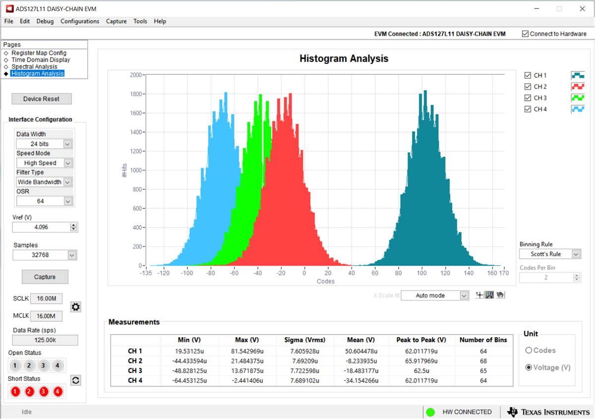
GUID-20220829-SS0I-G39Z-34X6-LKDGV1MF5DJD-low.png Figure 4-9 Histogram Plot of ADCs Inputs Shorted (Test Mode)

The ADC intrinsic voltage noise sigma is 7.7 μV, and offset of about 50 μV which is in line with the values in the ADS127L11 400-kSPS, Wide-Bandwidth, 24-Bit, Delta-Sigma ADC data sheet.

Next, short the front-end input (J8A, 2-3 = short).
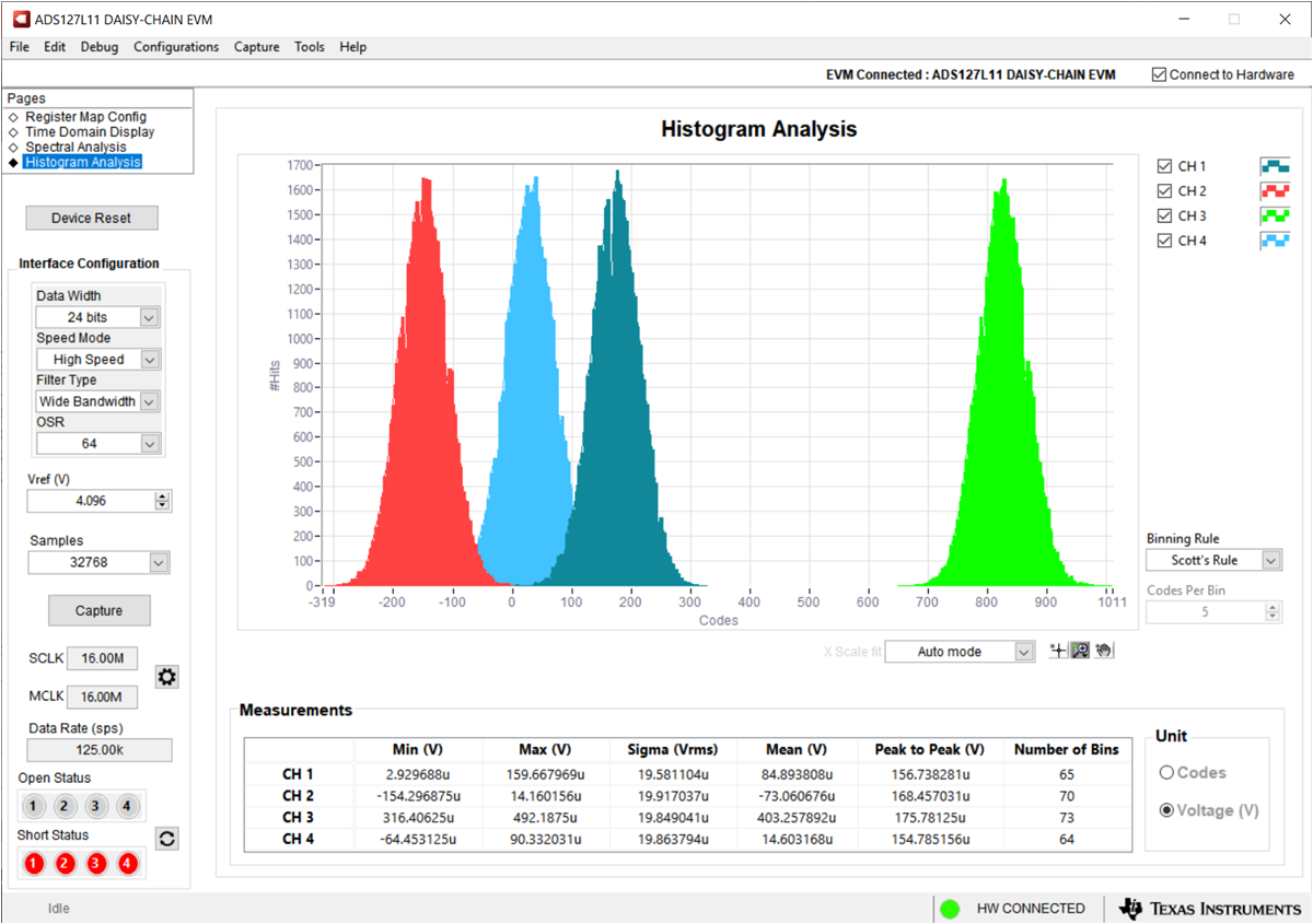
GUID-20220829-SS0I-NH86-9JWV-MLRBQK44VKT6-low.png Figure 4-10 Histogram Plot of Front-End Inputs Shorted

The full front-end voltage noise is around 19.8 μV, which is equivalent to 103 dB of Dynamic Range. The frequency plot in Figure 4-11 shows a clean spectrum with the highest tone at 94 dBFS.
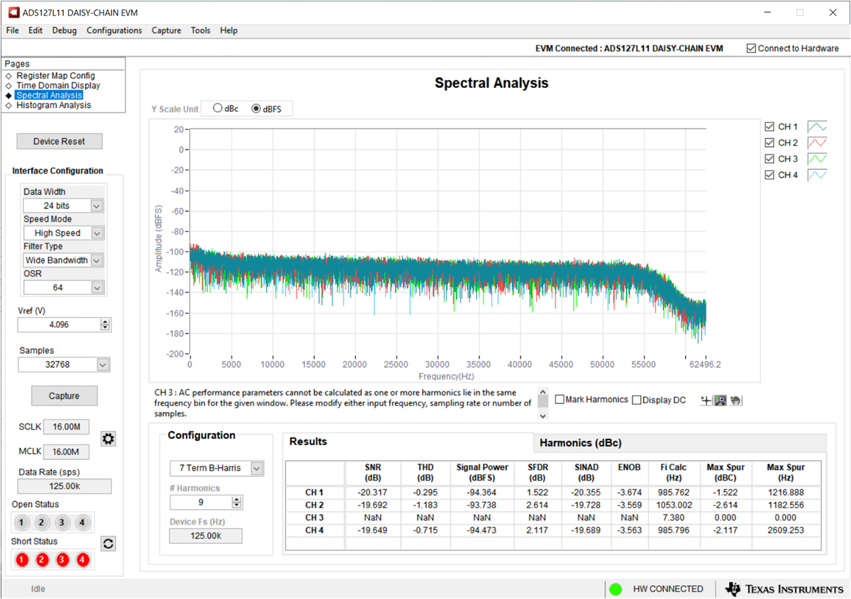
GUID-20220829-SS0I-BDQ0-ZS99-XLLFZ3PMCNHW-low.png Figure 4-11 Frequency-Domain Plot of Front-End Inputs Shorted

The time-domain plot (see Figure 4-12) verifies that there are no visible tones. The mean value of the channels are well below 0.5 mV which is the estimated offset of the whole channel including the offsets of OPA2320 (with gain of 4) and THS4551 (with gain of 2), and the ADS127L11 offset.
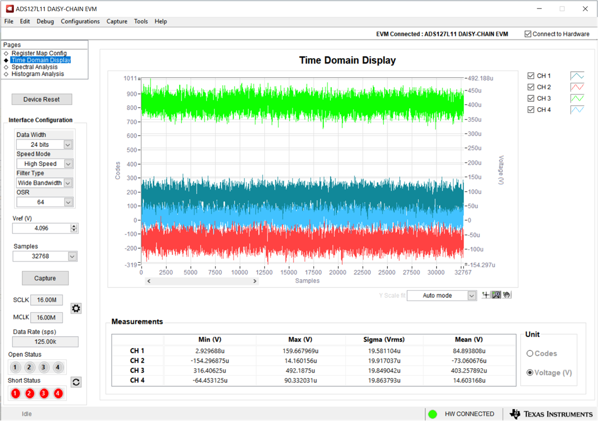
GUID-20220829-SS0I-V8JW-B3HM-DTBF8TQ5BM9C-low.png Figure 4-12 Time-Domain Plot of Front-End Inputs Shorted