JAJU882A December 2022 – January 2023
2.2.3 Additional Design Recommendations
- Comparator recommendations:
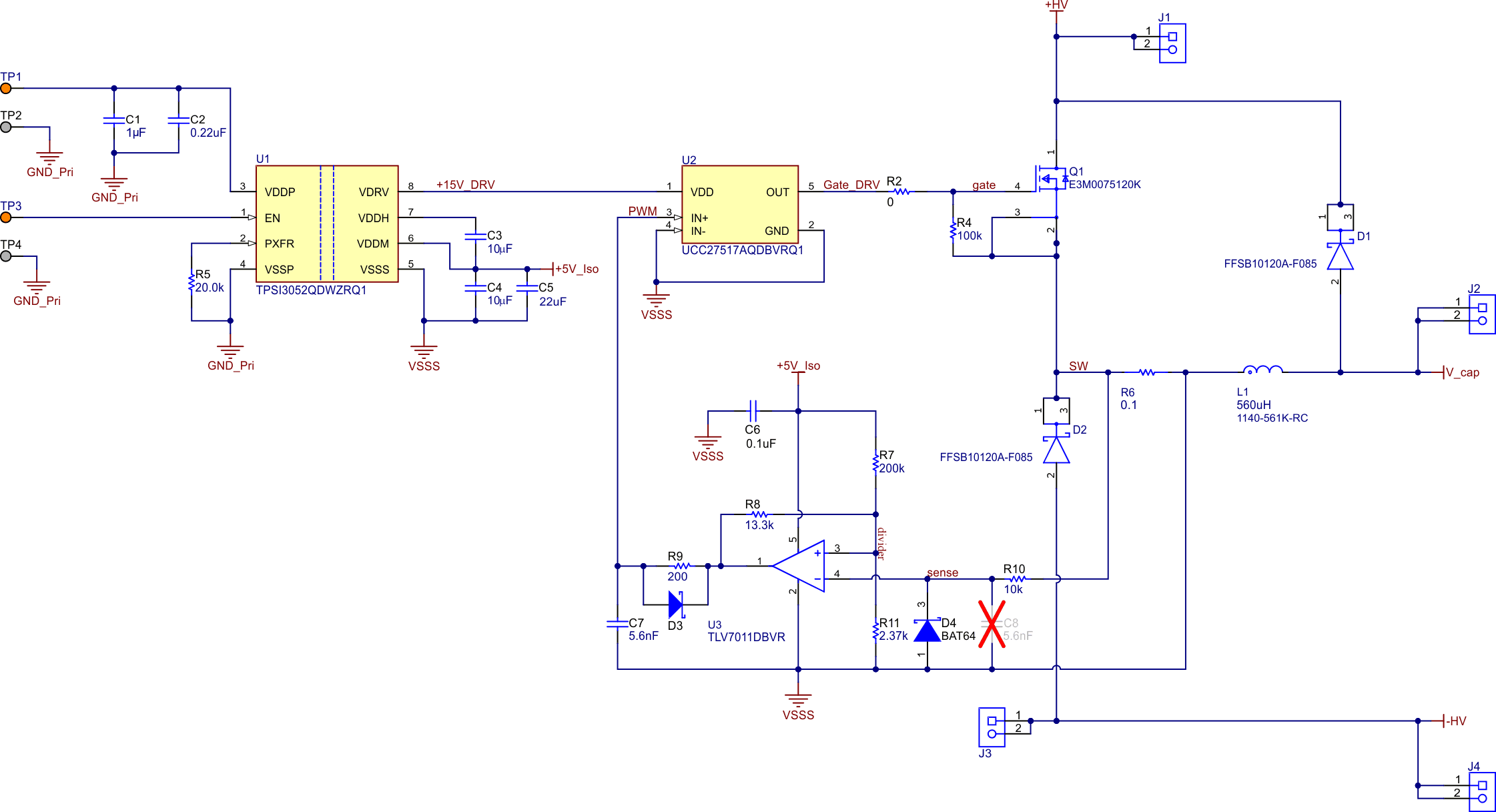
- When selecting the comparator for the design, ensure that it has a low supply current. The calculator previously provided for the TPSI3052-Q1 will help make sure that the TPSI3052-Q1 can supply power for this comparator and achieve the expected switching frequency. Power the comparator from VDDM (+5V) rail to consume less power.
- Do not load the output of the comparator and make sure to place an output resistance to limit the loading conditions. It is recommended to have a 200-Ω resistor between the comparator output and the FET driver input.
- At the input of the comparator it is recommended to include a fast-recovery Scottky diode and resistor to clamp any negative transient voltages generated from the inductor that might damage the input of the comparator.
- It is recommended to add a place holder for C8 to filter any high frequency noise that might falsely trigger the comparator
- Select R8 to be greater than 10-kΩ to minimize power dissipation
- For the inductor it is recommended to use a shielded inductor to minimize the noise produce by switching the inductor. In addition, it is critical to mention that the inductor used for this reference design is not an automotive qualified inductor. This reference design serves as a prove of concept and not a complete solution. However, the inductor is rated for the voltages and currents needed for the reference design.
- It is recommended to add D1 for testing purposes as shown in Figure 2-4. When the inductor is disconnected from the battery and left floating with the capacitor, this can result in oscillations at the output of the circuit. This concern was discovered during simulations.
- R9, C7, and D3 may be used if creating a forced minimum OFF-time is desired. This will reduce the maximum switching frequency, however it may also lead to DCM operation, which may cause ringing of the switch node at various frequencies, potentially affecting EMI performance. Adding this minimum off time may allow to reduce the inductance value, but may required a faster control loop.
It may be desired to block bidirectional current flow when precharge is disabled. The circuit shown can allow currents to flow back to the battery even when disabled due to the body diode of the FET. This current flow can be blocked by use of a standard precharge contactor in series with the MOSFET which also provides galvanic isolation. Alternatively, a FET can be placed in series with the switching FET between the RSHUNT and the inductor such that the source of this blocking FET is tied to VSSS and the gate tied to the TPSI3052-Q1 VDDH power supply. This allows the FET to be enabled while TPSI3052-Q1 is providing secondary power and the body diode is oriented to block reverse currents when disabled.
 Figure 2-4 Reference Design Schematics