SBAA390A June 2019 – September 2024 ADS8860 , OPA320 , REF6050
| REF6050 Input Voltage | Vref (Output of REF, Input on ADC) | AVDD (ADS8860) | DVDD (ADS8860) |
|---|---|---|---|
| 5.5V | 5.0V | 3.0V | 3.0V |
Design Description
This circuit document shows how the REF6050 (REF60xx series) voltage reference can be used to directly drive a switched capacitance ADC reference input pin. The reference input pin on many different types of data converters has a switched capacitor circuit that generates significant transient current requirements. These transients can have a significant impact in ADC accuracy, because the voltage reference must be settled to a constant accurate voltage. To respond to the transients on the ADC reference input, the voltage reference needs a wide-bandwidth buffer. The REF60xx series voltage reference incorporates an integrated wide-bandwidth buffer. This reference design will show measured ADC performance comparing a low-bandwidth reference to the wide-bandwidth REF6050. The document also covers alternative options for driving the ADC reference input.
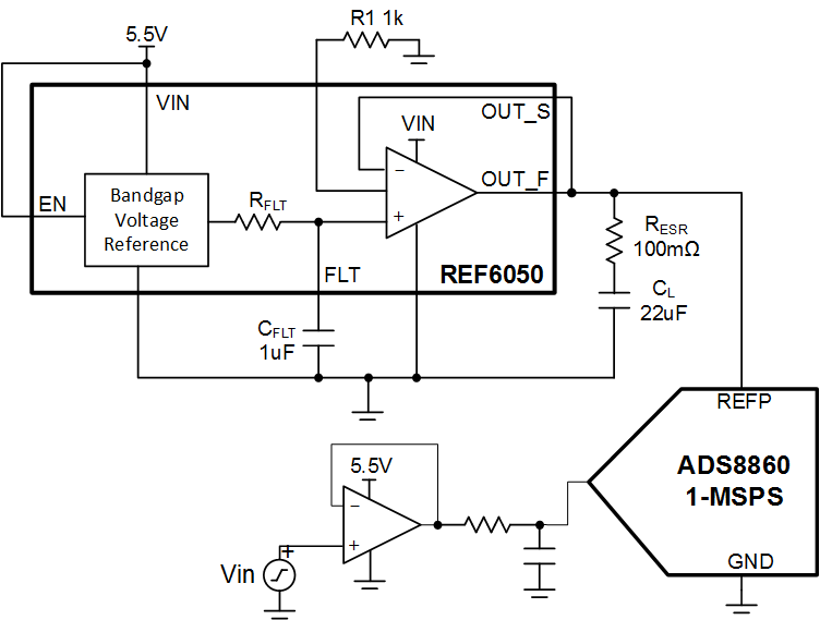
Specifications
| Specification (at 1MSPS) | Goal | Measured |
|---|---|---|
| THD | –108dB | –112.6dB |
| Reference Settling | 0 codes | 1.2 codes |
Design Notes
- This circuit can apply to many different data converters. See the data sheet to determine if a wide-bandwidth buffer is required. For devices that have a switched capacitor input, the REF60xx series reference is a good option because it has an integrated wide-bandwidth buffer. For data converters with an integrated wide-bandwidth buffer, the reference bandwidth is not important; therefore, consider other parameters such as reference noise and drift.
- See the REF60xx (REF6050) High-Precision Voltage Reference With Integrated ADC Drive Buffer Data Sheet for selecting the filter capacitors. In general, choosing larger capacitors helps to minimize noise. Also, the reference stability can be impacted by the Equivalent Series Resistance (ESR) of the capacitor.
- The topic of reference drive is covered in detail in the Driving the Reference Input on a SAR ADC video series from the TI Precision Labs - ADCs video training. The measurements shown in this reference design can be reproduced using the TI Precision Labs SAR ADC Evaluation Module Performance Demonstration Kit (PDK).
Wide-Bandwidth Buffer Inside the Reference
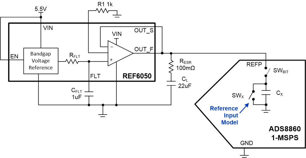
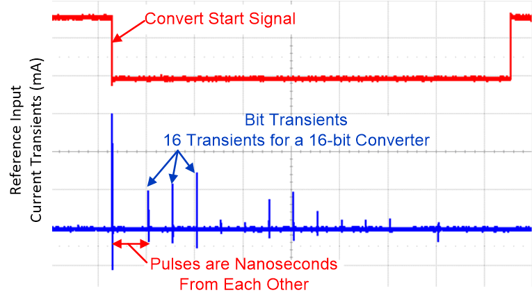
Many different data converters have a switched capacitor reference input. The following image shows a very simple model of this input. This model is for a traditional SAR ADC, but a similar model exists for some delta-sigma converters. In this example, a capacitance Cx is connected and disconnected from the external reference via SWBIT. The capacitor is reset with SWx after it is disconnected. This process is repeated N-times for an N-bit converter. This creates a large transient input current each time the capacitor is connected to the reference. The transient can be milliamps in amplitude, and the time between the transients is nanoseconds. The value of Cx changes throughout the conversion cycle, so the amplitude of the transients changes (see the following reference input graph). To get accurate conversion results, the reference voltage must rapidly respond to these transients. Thus, the reference requires a wide-bandwidth buffer to achieve the highest accuracy. Most references have an internal low bandwidth buffer which can be inadequate for the best performance. The REF6050 incorporates an internal wide-bandwidth buffer which is capable of responding to the transients present on most ADCs with a switched-capacitor reference input.
Wide-Bandwidth Buffer Inside the ADC
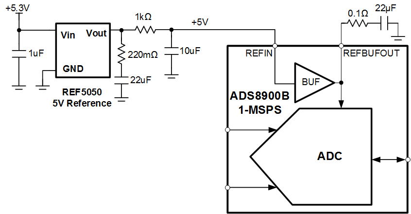
Some data converters have an internal wide-bandwidth buffer that is designed to drive the switched capacitor reference input. The input of this buffer is high impedance so the reference does not require a wide-bandwidth output. The ADS8900B and ADS8168 devices are examples of data converters that incorporate an integrated wide-bandwidth reference buffer.
Discrete Wide-Bandwidth Buffer Between Reference and ADC
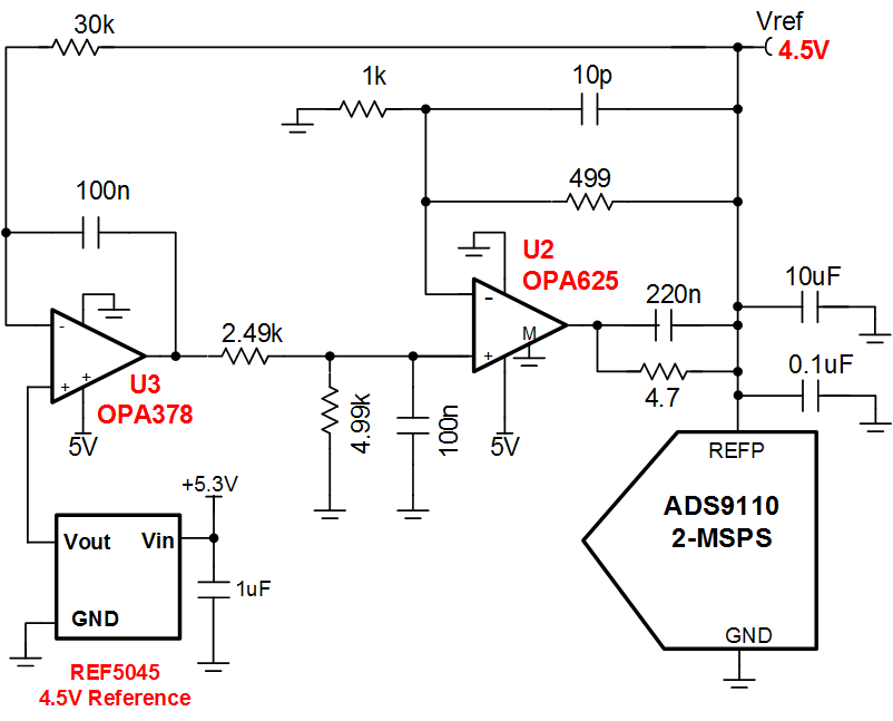
For devices that require a buffer, it is possible to build a discrete reference buffer rather than using a device with in integrated buffer (for example, REF6050). The following circuit shows a discrete buffer used on the ADS9110EVM-PDK. This circuit is a composite amplifier because it combines two amplifiers to form a circuit that has the benefit of both devices. The OPA378 has an ultra-low offset, and the OPA625 can respond to rapid transients.
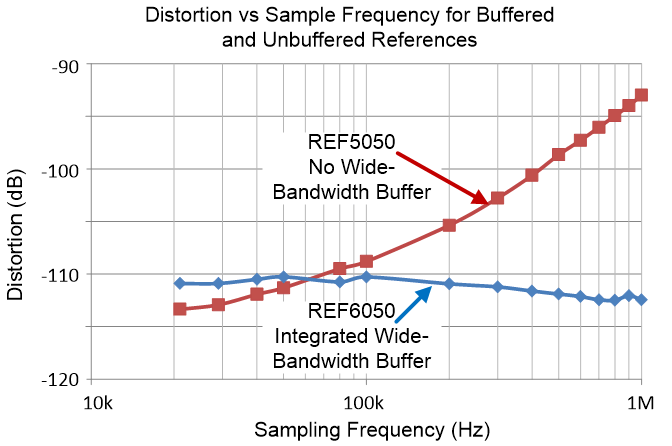
Distortion With and Without Reference Buffer Versus Sampling Rate
The following graph compares the distortion for an ADC with and without a wide-bandwidth reference buffer. Notice that for high sampling rates, the ADC with the wide-bandwidth buffer has substantially better THD performance. At low sampling rates, the buffer is less important because the reference has significant time to recover from the reference transients.
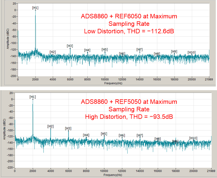
FFT With and Without Reference Buffer at 1MSPS
The following graphs show the FFT with and without the wide-bandwidth reference buffer at the maximum sampling rate (1MSPS). The graphs show that the harmonic distortion is clearly larger for the ADC without the wide-bandwidth buffer.
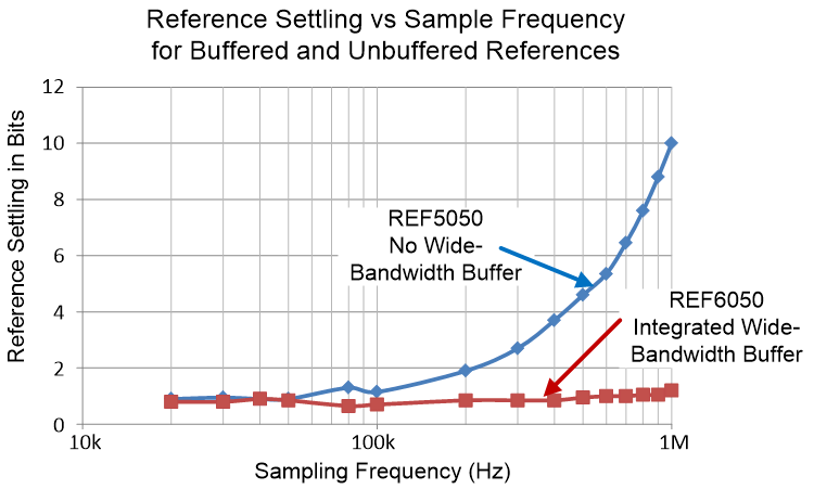
Reference Settling With and Without Reference Buffer Versus Sampling Rate
The following graph compares the settling performance to a DC signal for an ADC with and without a wide-bandwidth reference buffer. Settling performance indicates the error in the digitized result after one ADC conversion. In subsequent conversions, the ADC settling error will reduce for a constant DC input. Settling performance is very important in multiplexed systems, because it provides a good estimate of the types of error when switching channels. Notice that for high sampling rates, the ADC with the wide-bandwidth buffer has substantially better settling performance. At low sampling rates, the buffer is less important because the reference has significant time to recover from the reference transients.
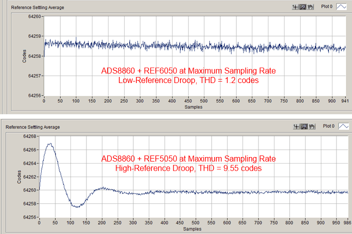
Reference Settling With and Without Reference Buffer Versus Time
The following graph shows the reference settling versus time at maximum sampling rate with a DC signal applied. Notice that for the unbuffered reference the signal has a significant transient settling error of 9.55 codes. This error requires about 300 samples to fully settle.
Design Featured Devices
| Device | Key Features | Link | Other Possible Devices |
|---|---|---|---|
| REF6050 | integrated ADC drive buffer, low output impedance: < 50mΩ (0–200kHz), excellent temperature drift performance 5ppm/°C (max) , extremely low noise total noise: 5µVRMS with 47µF capacitor | 5V, 5ppm/°C high-precision voltage reference with integrated buffer & enable pin | Voltage references |
| ADS8860 | 16-bit resolution, SPI, 1MSPS sample rate, single-ended input, VREF input range 2.5V to 5.0V | 16-bit, 1MSPS, 1-channel SAR ADC with single-ended input, SPI and daisy chain | Analog-to-digital converters (ADCs) |
| OPA320 | 20-MHz bandwidth, rail-to-rail with zero crossover distortion, VOS(MAX) = 150μV, VOS(Drift MAX) = 5μV/°C, en = 7nV/√ Hz | Precision, zero-crossover, 20MHz, 0.9pA Ib, RRIO, CMOS operational amplifier | Operational amplifiers (op amps) |