SBAS444E
May 2009 – December 2024
PRODUCTION DATA
1
1
Features
2
Applications
3
Description
Device Comparison Table
4
Pin Configuration and Functions
5
Specifications
5.1
Absolute Maximum Ratings
5.2
ESD Ratings
5.3
Recommended Operating Conditions
5.4
Thermal Information
5.5
Electrical Characteristics
5.6
Timing Requirements: I2C
5.7
Typical Characteristics
6
Parameter Measurement Information
6.1
Noise Performance
7
Detailed Description
7.1
Overview
7.2
Functional Block Diagrams
7.3
Feature Description
7.3.1
Multiplexer
7.3.2
Analog Inputs
7.3.3
Full-Scale Range (FSR) and LSB Size
7.3.4
Voltage Reference
7.3.5
Oscillator
7.3.6
Output Data Rate and Conversion Time
7.3.7
Digital Comparator (ADS1114 and ADS1115 Only)
7.3.8
Conversion Ready Pin (ADS1114 and ADS1115 Only)
7.3.9
SMbus Alert Response
7.4
Device Functional Modes
7.4.1
Reset and Power-Up
7.4.2
Operating Modes
7.4.2.1
Single-Shot Mode
7.4.2.2
Continuous-Conversion Mode
7.4.3
Duty Cycling For Low Power
7.5
Programming
7.5.1
I2C Interface
7.5.1.1
I2C Address Selection
7.5.1.2
I2C General Call
7.5.1.3
I2C Speed Modes
7.5.2
Target Mode Operations
7.5.2.1
Receive Mode
7.5.2.2
Transmit Mode
7.5.3
Writing To and Reading From the Registers
7.5.4
Data Format
8
Registers
8.1
Register Map
8.1.1
Address Pointer Register (address = N/A) [reset = N/A]
8.1.2
Conversion Register (P[1:0] = 00b) [reset = 0000h]
8.1.3
Config Register (P[1:0] = 01b) [reset = 8583h]
8.1.4
Lo_thresh (P[1:0] = 10b) [reset = 8000h] and Hi_thresh (P[1:0] = 11b) [reset = 7FFFh] Registers
9
Application and Implementation
9.1
Application Information
9.1.1
Basic Connections
9.1.2
Single-Ended Inputs
9.1.3
Input Protection
9.1.4
Unused Inputs and Outputs
9.1.5
Analog Input Filtering
9.1.6
Connecting Multiple Devices
9.1.7
Quick-Start Guide
9.2
Typical Application
9.2.1
Design Requirements
9.2.2
Detailed Design Procedure
9.2.2.1
Shunt Resistor Considerations
9.2.2.2
Operational Amplifier Considerations
9.2.2.3
ADC Input Common-Mode Considerations
9.2.2.4
Resistor (R1, R2, R3, R4) Considerations
9.2.2.5
Noise and Input Impedance Considerations
9.2.2.6
First-Order RC Filter Considerations
9.2.2.7
Circuit Implementation
9.2.2.8
Results Summary
9.2.3
Application Curves
10
Power Supply Recommendations
10.1
Power-Supply Sequencing
10.2
Power-Supply Decoupling
11
Layout
11.1
Layout Guidelines
11.2
Layout Example
12
Device and Documentation Support
12.1
Documentation Support
12.1.1
Related Documentation
12.2
Receiving Notification of Documentation Updates
12.3
Support Resources
12.4
Trademarks
12.5
Electrostatic Discharge Caution
12.6
Glossary
13
Revision History
14
Mechanical, Packaging, and Orderable Information
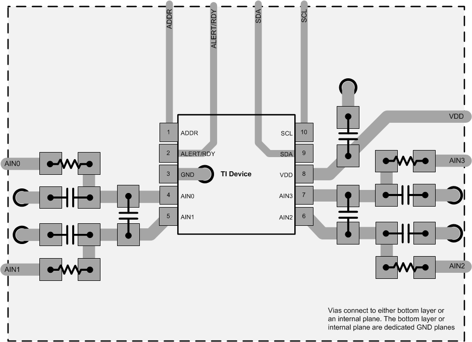
11.2
Layout Example
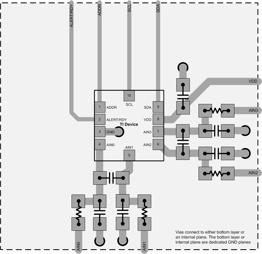
Figure 11-2
ADS1115 X2QFN Package
Figure 11-3
ADS1115 VSSOP Package