-
ADS129x Low-Power, 8-Channel, 24-Bit Analog Front-End for Biopotential Measurements
- 1 Features
- 2 Applications
- 3 Description
- 4 Revision History
- 5 Device Comparison
- 6 Pin Configuration and Functions
- 7 Specifications
- 8 Parameter Measurement Information
-
9 Detailed Description
- 9.1 Overview
- 9.2 Functional Block Diagram
- 9.3
Feature Description
- 9.3.1
Analog Functionality
- 9.3.1.1 EMI Filter
- 9.3.1.2 Analog Input Structure
- 9.3.1.3
Input Multiplexer
- 9.3.1.3.1 Device Noise Measurements
- 9.3.1.3.2 Test Signals (TestP and TestN)
- 9.3.1.3.3 Auxiliary Differential Input (TESTP_PACE_OUT1, TESTN_PACE_OUT2)
- 9.3.1.3.4 Temperature Sensor (TempP, TempN)
- 9.3.1.3.5 Supply Measurements (MVDDP, MVDDN)
- 9.3.1.3.6 Lead-Off Excitation Signals (LoffP, LoffN)
- 9.3.1.3.7 Auxiliary Single-Ended Input
- 9.3.1.4 Analog Input
- 9.3.1.5 PGA Settings and Input Range
- 9.3.1.6 Reference
- 9.3.1.7
ECG-Specific Functions
- 9.3.1.7.1 Input Multiplexer (Rerouting The Right Leg Drive Signal)
- 9.3.1.7.2 Input Multiplexer (Measuring The Right Leg Drive Signal)
- 9.3.1.7.3 Wilson Central Terminal (WCT) and Chest Leads
- 9.3.1.7.4 Lead-Off Detection
- 9.3.1.7.5 RLD Lead-Off
- 9.3.1.7.6 Right Leg Drive (RLD) DC Bias Circuit
- 9.3.1.7.7 Pace Detect
- 9.3.1.7.8 Respiration
- 9.3.2 Digital Functionality
- 9.3.1
Analog Functionality
- 9.4 Device Functional Modes
- 9.5
Programming
- 9.5.1 SPI Interface
- 9.5.2
SPI Command Definitions
- 9.5.2.1 WAKEUP: Exit Standby Mode
- 9.5.2.2 STANDBY: Enter Standby Mode
- 9.5.2.3 RESET: Reset Registers to Default Values
- 9.5.2.4 START: Start Conversions
- 9.5.2.5 STOP: Stop Conversions
- 9.5.2.6 RDATAC: Read Data Continuous
- 9.5.2.7 SDATAC: Stop Read Data Continuous
- 9.5.2.8 RDATA: Read Data
- 9.5.2.9 Sending Multibyte Commands
- 9.5.2.10 RREG: Read From Register
- 9.5.2.11 WREG: Write to Register
- 9.6
Register Maps
- 9.6.1
Register Descriptions
- 9.6.1.1 ID: ID Control Register (address = 00h) (reset = xxh)
- 9.6.1.2 CONFIG1: Configuration Register 1 (address = 01h) (reset = 06h)
- 9.6.1.3 CONFIG2: Configuration Register 2 (address = 02h) (reset = 40h)
- 9.6.1.4 CONFIG3: Configuration Register 3 (address = 03h) (reset = 40h)
- 9.6.1.5 LOFF: Lead-Off Control Register (address = 04h) (reset = 00h)
- 9.6.1.6 CHnSET: Individual Channel Settings (n = 1 to 8) (address = 05h to 0Ch) (reset = 00h)
- 9.6.1.7 RLD_SENSP: RLD Positive Signal Derivation Register (address = 0Dh) (reset = 00h)
- 9.6.1.8 RLD_SENSN: RLD Negative Signal Derivation Register (address = 0Eh) (reset = 00h)
- 9.6.1.9 LOFF_SENSP: Positive Signal Lead-Off Detection Register (address = 0Fh) (reset = 00h)
- 9.6.1.10 LOFF_SENSN: Negative Signal Lead-Off Detection Register (address = 10h) (reset = 00h)
- 9.6.1.11 LOFF_FLIP: Lead-Off Flip Register (address = 11h) (reset = 00h)
- 9.6.1.12 LOFF_STATP: Lead-Off Positive Signal Status Register (address = 12h) (reset = 00h)
- 9.6.1.13 LOFF_STATN: Lead-Off Negative Signal Status Register (address = 13h) (reset = 00h)
- 9.6.1.14 GPIO: General-Purpose I/O Register (address = 14h) (reset = 0Fh)
- 9.6.1.15 PACE: Pace Detect Register (address = 15h) (reset = 00h)
- 9.6.1.16 RESP: Respiration Control Register (address = 16h) (reset = 00h)
- 9.6.1.17 CONFIG4: Configuration Register 4 (address = 17h) (reset = 00h)
- 9.6.1.18 WCT1: Wilson Central Terminal and Augmented Lead Control Register (address = 18h) (reset = 00h)
- 9.6.1.19 WCT2: Wilson Central Terminal Control Register (address = 18h) (reset = 00h)
- 9.6.1
Register Descriptions
- 10Application and Implementation
- 11Power Supply Recommendations
- 12Layout
- 13Device and Documentation Support
- 14Mechanical, Packaging, and Orderable Information
- IMPORTANT NOTICE
ADS129x Low-Power, 8-Channel, 24-Bit Analog Front-End for Biopotential Measurements
1 Features
- Eight Low-Noise PGAs and Eight High-Resolution ADCs (ADS1298, ADS1298R)
- Low Power: 0.75 mW/channel
- Input-Referred Noise: 4 μVPP (150 Hz BW, G = 6)
- Input Bias Current: 200 pA
- Data Rate: 250 SPS to 32 kSPS
- CMRR: –115 dB
- Programmable Gain: 1, 2, 3, 4, 6, 8, or 12
- Supports systems meeting AAMI EC11, EC13, IEC60601-1, IEC60601-2-27, and IEC60601-2-51 Standards
- Unipolar or Bipolar Supplies:
- AVDD = 2.7 V to 5.25 V
- DVDD = 1.65 V to 3.6 V
- Built-In Right Leg Drive Amplifier, Lead-Off Detection, Wilson Center Terminal, Pace Detection, Test Signals
- Integrated Respiration Impedance Measurement
- Digital Pace Detection Capability
- Built-In Oscillator and Reference
- SPI™-Compatible Serial Interface
2 Applications
- Medical Instrumentation (ECG, EMG, and EEG):
Patient Monitoring; Holter, Event, Stress, and Vital Signs Including ECG, AED, Telemedicine
Bispectral Index (BIS), Evoked Audio Potential (EAP), Sleep Study Monitor
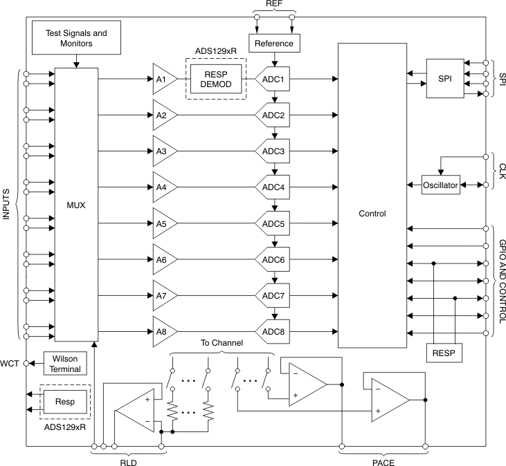
Simplified Schematic
3 Description
The ADS1294, ADS1296, ADS1298 (ADS129x) and ADS1294R, ADS1296R ADS1298R (ADS129xR) are a family of multichannel, simultaneous sampling,
24-bit, delta-sigma (ΔΣ) analog-to-digital converters (ADCs) with built-in programmable gain amplifiers (PGAs), internal reference, and an onboard oscillator. The ADS129x and ADS129xR incorporate all of the features that are commonly required in medical electrocardiogram (ECG) and electroencephalogram (EEG) applications. With high levels of integration and exceptional performance, the ADS129x and ADS129xR enables the development of scalable medical instrumentation systems at significantly reduced size, power, and overall cost.
The ADS129x and ADS129xR have a flexible input multiplexer (mux) per channel that can be independently connected to the internally-generated signals for test, temperature, and lead-off detection. Additionally, any configuration of input channels can be selected for derivation of the right leg drive (RLD) output signal. The ADS129x and ADS129xR operate at data rates as high as 32 kSPS, thereby allowing the implementation of software pace detection. Lead-off detection can be implemented internal to the device, either with a pullup or pulldown resistor, or an excitation current sink or source. Three integrated amplifiers generate the Wilson central terminal (WCT) and the Goldberger central terminals (GCT) required for a standard 12-lead ECG. The ADS129xR versions include a fully integrated, respiration impedance measurement function. Multiple ADS129x and ADS129xR devices can be cascaded in high channel count systems in a daisy-chain configuration.
Package options include a tiny 8-mm × 8-mm,
64-ball BGA, and a TQFP-64. The ADS129x BGA version is specified over the commercial temperature range of 0°C to 70°C. The ADS129xR BGA and ADS129x TQFP versions are specified over the industrial temperature range of –40°C to +85°C.
Device Information(1)
| PART NUMBER | PACKAGE | BODY SIZE (NOM) |
|---|---|---|
| ADS129x, ADS129xR | NFBGA (64) | 8.00 mm × 8.00 mm |
| TQFP (64) | 10.00 mm × 10.00 mm |
- For all available packages, see the package option addendum at the end of the data sheet.
4 Revision History
Changes from J Revision (January 2014) to K Revision
- Added ESD Ratings table, Feature Description section, Device Functional Modes, Application and Implementation section, Power Supply Recommendations section, Layout section, Device and Documentation Support section, and Mechanical, Packaging, and Orderable Information section Go
- Changed text throughout data sheet for clarityGo
- Added note to DAISY_IN pin Go
- Added note to DAISY_IN pin Go
- Changed Equation 3Go
Changes from I Revision (January 2012) to J Revision
- Changed NC pin discription in Pin Assignments tableGo
- Changed NC pin discription in Pin Assignments tableGo
- Added graph of INTERNAL VREF DRIFT vs TEMPERATUREGo
- Changed order of subsections in the Theory of Operation sectionGo
- Changed single-ended input description to correct input range valuesGo
- Changed Figure 27 to show correct input range for single-ended inputsGo
- Changed Figure 28 to show correct input range for single-ended inputsGo
- Deleted text regarding large scale signalGo
- Changed Figure 32 to provide a more stable external reference driver circuitGo
- Updated Figure 57Go
- Added Figure 58Go
- Added discussion of SCLK/DRDY bus behavior to Data Ready (DRDY) sectionGo
- Added Figure 60Go
- Added status Word section and Figure 61 to discuss the status wordGo
- Added Readback Length sectionGo
- Added SCLK Clocking Methods sectionGo
- Changed units in TEST_AMP bit description in CONFIG2 registerGo
- Changed Figure 93 to clarify Initial Flow at Power-UpGo
- Changed Power-Up Sequencing section text to clarify start-up timingGo
- Changed Figure 105Go
- Changed power-up reset wait time in Table 38Go
Changes from H Revision (October 2011) to I Revision
- Added eighth Features bullet (list of standards supported)Go
- Updated BGA pin outGo
- Deleted duplicate Digital input voltage and Digital output voltage rows from Absolute Maximum Ratings tableGo
- Changed parameter name of Channel Performance, Common-mode rejection ratio and Power-supply rejection ratio parameters in Electrical Characteristics tableGo
- Updated Functional Block DiagramGo
- Updated description of Analog Input sectionGo
- Updated Figure 30Go
- Updated Figure 33Go
- Updated Figure 34Go
- Changed description of START pin in START sectionGo
- Changed description of Data Ready (DRDY) sectionGo
- Changed conversion description in Single-Shot Mode sectionGo
- Changed conversion description in Continuous Mode sectionGo
- Changed Unit column in Table 14Go
- Added power-down recommendation to bit 7 description of CHnSET: Individual Channel Settings sectionGo
- Changed description of bit 5 in RESP: Respiration Control Register sectionGo
- Corrected name of bit 6 in WCT2: Wilson Central Terminal Control Register sectionGo
Changes from G Revision (February 2011) to H Revision
- Changed footnote 1 of BGA Pin Assignments tableGo
- Added footnote 1 cross-reference to RLDIN, TESTP_PACE_OUT1, and TESTP_PACE_OUT in BGA Pin Assignments tableGo
- Changed footnote 1 of PAG Pin Assignments tableGo
- Added footnote 1 cross-reference to TESTP_PACE_OUT1, TESTP_PACE_OUT2, and RLDIN in PAG Pin Assignments tableGo
- Changed description of AVSS and AVDD in PAG Pin Assignments tableGo
- Added (ADS1298) to High-Resolution mode and Low-Power mode test conditions of Supply Current section in Electrical Characteristics tableGo
- Changed 3-V Power Dissipation, Quiescent channel power test conditions in Electrical Characteristics tableGo
- Changed 5-V Power Dissipation, Quiescent channel power test conditions in Electrical Characteristics tableGo
- Changed title of Figure 20Go
- Updated Figure 42Go
- Added new paragraph to Respiration sectionGo
- Updated Equation 5Go
- Changed title of Table 13Go
- Updated Figure 66Go
- Changed description of STANDBY: Enter STANDBY Mode sectionGo
- Changed bit name for bits 5, 6, and 7 in ID register of Table 16Go
- Changed bit name for bits 5, 6, and 7 in ID: ID Control Register sectionGo
- Added footnote to Figure 97Go
- Changed description of solid ceramic capacitor in Power Supplies and Grounding sectionGo
- Changed description of Connecting the Device to Bipolar (±1.5 V/1.8 V) Supplies sectionGo
Changes from F Revision (October 2010) to G Revision
- Updated entire document to include ADS1294R, ADS1296R, and ADS1298R devicesGo
- Added CONFIG2.WCT_CHOP bit functionality to Wilson Central Terminal (WCT) and Chest Leads sectionGo
- Added CONFIG2.WCT_CHOP bit functionality to CONFIG2: Configuration Register 2Go
- Corrected TEST_PACE_OUT1 and TEST_PACE_OUT2 description in PACE: PACE Detect RegisterGo
5 Device Comparison
| PRODUCT | PACKAGE OPTIONS | OPERATING TEMPERATURE RANGE | RESPIRATION CIRCUITRY | CHANNELS | ADC RESOLUTION | MAXIMUM SAMPLING RATE |
|---|---|---|---|---|---|---|
| ADS1194 | TQFP-64 | 0°C to 70°C | No | 4 | 16 | 8 kSPS |
| NFBGA-64 | 0°C to 70°C | |||||
| ADS1196 | TQFP-64 | 0°C to 70°C | No | 6 | 16 | 8 kSPS |
| NFBGA-64 | 0°C to 70°C | |||||
| ADS1198 | TQFP-64 | 0°C to 70°C | No | 8 | 16 | 8 kSPS |
| NFBGA-64 | 0°C to 70°C | |||||
| ADS1294 | TQFP-64 | –40°C to +85°C | External | 4 | 24 | 32 kSPS |
| NFBGA-64 | 0°C to 70°C | |||||
| ADS1294R | NFBGA-64 | –40°C to +85°C | Yes | |||
| ADS1296 | TQFP-64 | –40°C to +85°C | External | 6 | 24 | 32 kSPS |
| NFBGA-64 | 0°C to 70°C | |||||
| ADS1296R | NFBGA-64 | –40°C to +85°C | Yes | |||
| ADS1298 | TQFP-64 | –40°C to +85°C | External | 8 | 24 | 32 kSPS |
| NFBGA-64 | 0°C to 70°C | |||||
| ADS1298R | NFBGA-64 | –40°C to +85°C | Yes |
6 Pin Configuration and Functions
Pin Function: NFBGA Package
| PIN | TYPE | DESCRIPTION | |
|---|---|---|---|
| NO. | NAME | ||
| 1A | IN8P(1) | Analog input | Differential analog positive input 8 (ADS1298 and ADS1298R) |
| 1B | IN7P(1) | Analog input | Differential analog positive input 7 (ADS1298 and ADS1298R) |
| 1C | IN6P(1) | Analog input | Differential analog positive input 6 (ADS1296, ADS1298, ADS1296R, ADS1298R) |
| 1D | IN5P(1) | Analog input | Differential analog positive input 5 (ADS1296, ADS1298, ADS1296R, ADS1298R) |
| 1E | IN4P(1) | Analog input | Differential analog positive input 4 |
| 1F | IN3P(1) | Analog input | Differential analog positive input 3 |
| 1G | IN2P(1) | Analog input | Differential analog positive input 2 |
| 1H | IN1P(1) | Analog input | Differential analog positive input 1 |
| 2A | IN8N(1) | Analog input | Differential analog negative input 8 (ADS1298, ADS1298R) |
| 2B | IN7N(1) | Analog input | Differential analog negative input (ADS1298, ADS1298R) |
| 2C | IN6N(1) | Analog input | Differential analog negative input 6 (ADS1296, ADS1298, ADS1296R, ADS1298R) |
| 2D | IN5N(1) | Analog input | Differential analog negative input 5 (ADS1296, ADS1298, ADS1296R, ADS1298R) |
| 2E | IN4N(1) | Analog input | Differential analog negative input 4 |
| 2F | IN3N(1) | Analog input | Differential analog negative input 3 |
| 2G | IN2N(1) | Analog input | Differential analog negative input 2 |
| 2H | IN1N(1) | Analog input | Differential analog negative input 1 |
| 3A | RLDIN(1) | Analog input | Right leg drive input to mux |
| 3B | RLDOUT | Analog output | Right leg drive output |
| 3C | RLDINV | Analog input/output | Right leg drive inverting input |
| 3D | WCT | Analog output | Wilson central terminal output |
| 3E | TESTP_PACE_OUT1(1) | Analog input/buffer output | Internal test signal or single-ended buffer output based on register settings |
| 3F | TESTN_PACE_OUT2(1) | Analog input/output | Internal test signal or single-ended buffer output based on register settings |
| 3G | VCAP4 | — | Analog bypass capacitor; connect 1-μF capacitor to AVSS |
| 3H | VREFP | Analog input/output | Positive reference input/output voltage |
| 4A | AVDD | Supply | Analog supply |
| 4B | AVDD | Supply | Analog supply |
| 4C | RLDREF | Analog input | Right leg drive noninverting input |
| 4D | AVSS | Supply | Analog ground |
| 4E | RESV1 | Digital input | Reserved for future use; must tie to logic low (DGND). |
| 4F | RESP_MODN | Analog output | ADS129xR: modulation clock for respiration measurement, negative side. ADS129x: leave floating. |
| 4G | RESP_MODP | Analog output | ADS129xR: modulation clock for respiration measurement, positive side. ADS129x: leave floating. |
| 4H | VREFN | Analog input | Negative reference voltage |
| 5A | AVSS | Supply | Analog ground |
| 5B | AVSS | Supply | Analog ground |
| 5C | AVSS | Supply | Analog ground |
| 5D | AVSS | Supply | Analog ground |
| 5E | GPIO4 | Digital input/output | General-purpose input/output pin 4 |
| 5F | GPIO1 | Digital input/output | General-purpose input/output pin 1 |
| 5G | PWDN | Digital input | Power-down pin; active low |
| 5H | VCAP1 | — | Analog bypass capacitor; connect 22-μF capacitor to AVSS |
| 6A | AVDD | Supply | Analog supply |
| 6B | AVDD | Supply | Analog supply |
| 6C | AVDD | Supply | Analog supply |
| 6D | DRDY | Digital output | Data ready; active low |
| 6E | GPIO3 | Digital input/output | General purpose input/output pin 3 |
| 6F | DAISY_IN(2) | Digital input | Daisy-chain input; if not used, short to DGND. |
| 6G | RESET | Digital input | System-reset pin; active low |
| 6H | VCAP2 | — | Analog bypass capacitor; connect 1-μF capacitor to AVSS |
| 7A | AVDD1 | Supply | Analog supply for charge pump |
| 7B | VCAP3 | — | Analog bypass capacitor; internally generated AVDD + 1.9 V; connect 1-μF capacitor to AVSS |
| 7C | DGND | Supply | Digital ground |
| 7D | DGND | Supply | Digital ground |
| 7E | GPIO2 | Digital input/output | General-purpose input/output pin 2 |
| 7F | CS | Digital input | SPI chip select; active low |
| 7G | START | Digital input | Start conversion |
| 7H | DGND | Supply | Digital ground |
| 8A | AVSS1 | Supply | Analog ground for charge pump |
| 8B | CLKSEL | Digital input | Master clock select |
| 8C | DVDD | Supply | Digital power supply |
| 8D | DVDD | Supply | Digital power supply |
| 8E | DOUT | Digital output | SPI data output |
| 8F | SCLK | Digital input | SPI clock |
| 8G | CLK | Digital input/output | External Master clock input or internal clock output. |
| 8H | DIN | Digital input | SPI data input |

Pin Functions: TQFP Package
| PIN | TYPE | DESCRIPTION | |
|---|---|---|---|
| NO. | NAME | ||
| 1 | IN8N(1) | Analog input | Differential analog negative input 8 (ADS1298) |
| 2 | IN8P(1) | Analog input | Differential analog positive input 8 (ADS1298) |
| 3 | IN7N(1) | Analog input | Differential analog negative input 7 (ADS1298) |
| 4 | IN7P(1) | Analog input | Differential analog positive input 7 (ADS1298) |
| 5 | IN6N(1) | Analog input | Differential analog negative input 6 (ADS1296, ADS1298) |
| 6 | IN6P(1) | Analog input | Differential analog positive input 6 (ADS1296, ADS1298) |
| 7 | IN5N(1) | Analog input | Differential analog negative input 5 (ADS1296, ADS1298) |
| 8 | IN5P(1) | Analog input | Differential analog positive input 5 (ADS1296, ADS1298) |
| 9 | IN4N(1) | Analog input | Differential analog negative input 4 |
| 10 | IN4P(1) | Analog input | Differential analog positive input 4 |
| 11 | IN3N(1) | Analog input | Differential analog negative input 3 |
| 12 | IN3P(1) | Analog input | Differential analog positive input 3 |
| 13 | IN2N(1) | Analog input | Differential analog negative input 2 |
| 14 | IN2P(1) | Analog input | Differential analog positive input 2 |
| 15 | IN1N(1) | Analog input | Differential analog negative input 1 |
| 16 | IN1P(1) | Analog input | Differential analog positive input 1 |
| 17 | TESTP_PACE_OUT1(1) | Analog input/buffer output | Internal test signal/single-ended buffer output based on register settings |
| 18 | TESTN_PACE_OUT2(1) | Analog input/output | Internal test signal/single-ended buffer output based on register settings |
| 19 | AVDD | Supply | Analog supply |
| 20 | AVSS | Supply | Analog ground |
| 21 | AVDD | Supply | Analog supply |
| 22 | AVDD | Supply | Analog supply |
| 23 | AVSS | Supply | Analog ground |
| 24 | VREFP | Analog input/output | Positive reference input/output voltage |
| 25 | VREFN | Analog input | Negative reference voltage |
| 26 | VCAP4 | — | Analog bypass capacitor; connect 1-μF capacitor to AVSS |
| 27 | NC | — | No connection, can be connected to AVDD or AVSS with a 10-kΩ resistor |
| 28 | VCAP1 | — | Analog bypass capacitor; connect 22-μF capacitor to AVSS |
| 29 | NC | — | No connection, can be connected to AVDD or AVSS with a 10-kΩ resistor |
| 30 | VCAP2 | — | Analog bypass capacitor; connect 1-μF capacitor to AVSS |
| 31 | RESV1 | Digital input | Reserved for future use; must tie to logic low (DGND). |
| 32 | AVSS | Supply | Analog ground |
| 33 | DGND | Supply | Digital ground |
| 34 | DIN | Digital input | SPI data input |
| 35 | PWDN | Digital input | Power-down pin; active low |
| 36 | RESET | Digital input | System-reset pin; active low |
| 37 | CLK | Digital input/output | External Master clock input or internal clock output. |
| 38 | START | Digital input | Start conversion |
| 39 | CS | Digital input | SPI chip select; active low |
| 40 | SCLK | Digital input | SPI clock |
| 41 | DAISY_IN(2) | Digital input | Daisy-chain input; if not used, short to DGND. |
| 42 | GPIO1 | Digital input/output | General-purpose input/output pin 1 |
| 43 | DOUT | Digital output | SPI data output |
| 44 | GPIO2 | Digital input/output | General-purpose input/output pin 2 |
| 45 | GPIO3 | Digital input/output | General-purpose input/output pin 3 |
| 46 | GPIO4 | Digital input/output | General-purpose input/output pin 4 |
| 47 | DRDY | Digital output | Data ready; active low |
| 48 | DVDD | Supply | Digital power supply |
| 49 | DGND | Supply | Digital ground |
| 50 | DVDD | Supply | Digital power supply |
| 51 | DGND | Supply | Digital ground |
| 52 | CLKSEL | Digital input | Master clock select |
| 53 | AVSS1 | Supply | Analog ground |
| 54 | AVDD1 | Supply | Analog supply |
| 55 | VCAP3 | — | Analog bypass capacitor; internally generated AVDD + 1.9 V; connect 1-μF capacitor to AVSS |
| 56 | AVDD | Supply | Analog supply |
| 57 | AVSS | Supply | Analog ground |
| 58 | AVSS | Supply | Analog ground |
| 59 | AVDD | Supply | Analog supply |
| 60 | RLDREF | Analog input | Right leg drive noninverting input |
| 61 | RLDINV | Analog input/output | Right leg drive inverting input |
| 62 | RLDIN(1) | Analog input | Right leg drive input to mux |
| 63 | RLDOUT | Analog output | Right leg drive output |
| 64 | WCT | Analog output | Wilson Central Terminal output |
7 Specifications
7.1 Absolute Maximum Ratings
over operating free-air temperature range (unless otherwise noted)(1)7.2 ESD Ratings
| VALUE | UNIT | |||
|---|---|---|---|---|
| V(ESD) | Electrostatic discharge | Human body model (HBM), per ANSI/ESDA/JEDEC JS-001, all pins(1) | ±2000 | V |
| Charged device model (CDM), per JEDEC specification JESD22-C101, all pins(2) | ±500 | |||
7.3 Recommended Operating Conditions
over operating ambient temperature range (unless otherwise noted)| MIN | NOM | MAX | UNIT | ||
|---|---|---|---|---|---|
| POWER SUPPLY | |||||
| Analog power supply (AVDD – AVSS) | 2.7 | 3 | 5.25 | V | |
| Digital power supply (DVDD) | 1.65 | 1.8 | 3.6 | V | |
| AVDD – DVDD | –2.1 | 3.6 | V | ||
| ANALOG INPUTS | |||||
| Full-scale differential input voltage range (AINP – AINN) | ±VREF / Gain | V | |||
| Common-mode input voltage | See the Input Common-Mode Range subsection of the PGA Settings and Input Range section | ||||
| VOLTAGE REFERENCE INPUTS | |||||
| Differential reference voltage | 3-V supply VREF = (VREFP – VREFN) | 2.5 | V | ||
| 5-V supply VREF = (VREFP – VREFN) | 4 | V | |||
| Negative input (VREFN) | AVSS | V | |||
| Positive input (VREFP) | AVSS + 2.5 | V | |||
| CLOCK INPUT | |||||
| External clock input frequency | CLKSEL pin = 0 | 1.94 | 2.048 | 2.25 | MHz |
| DIGITAL INPUTS | |||||
| Input Voltage | DGND | DVDD | V | ||
| TEMPERATURE RANGE | |||||
| Operating temperature range | Commercial grade | 0 | 70 | °C | |
| Industrial grade | –40 | 85 | °C | ||
7.4 Thermal Information
| THERMAL METRIC(1) | ADS129x, ADS129xR | UNIT | ||
|---|---|---|---|---|
| PAG (TQFP) | ZXG (NFBGA) | |||
| 64 PINS | 64 PINS | |||
| RθJA | Junction-to-ambient thermal resistance | 35 | 48 | °C/W |
| RθJC(top) | Junction-to-case (top) thermal resistance | 31 | 8 | °C/W |
| RθJB | Junction-to-board thermal resistance | 26 | 25 | °C/W |
| ψJT | Junction-to-top characterization parameter | 0.1 | 0.5 | °C/W |
| ψJB | Junction-to-board characterization parameter | N/A | 22 | °C/W |
7.5 Electrical Characteristics
Min and max specifications apply for all commercial grade (TA = 0°C to 70°C) devices, and from TA = –40°C to +85°C for industrial-grade devices. Typical specifications at TA = 25°C. All specifications at DVDD = 1.8 V, AVDD – AVSS = 3 V(3),VREF = 2.4 V, external fCLK = 2.048 MHz, data rate = 500 SPS, HR mode(6), and gain = 6 (unless otherwise noted).
| PARAMETER | TEST CONDITIONS | MIN | TYP | MAX | UNIT | |||
|---|---|---|---|---|---|---|---|---|
| ANALOG INPUTS | ||||||||
| Input capacitance | 20 | pF | ||||||
| Input bias current | TA = 25°C, input = 1.5 V | ±200 | pA | |||||
| TA = 0°C to 70°C, input = 1.5 V | ±1 | nA | ||||||
| TA = –40°C to +85°C, input = 1.5 V | ±1.2 | nA | ||||||
| DC input impedance | No lead-off | 1000 | MΩ | |||||
| Current source lead-off detection | 500 | MΩ | ||||||
| Pullup resistor lead-off detection | 10 | MΩ | ||||||
| PGA PERFORMANCE | ||||||||
| Gain settings | 1, 2, 3, 4, 6, 8, 12 | |||||||
| Bandwidth | See Table 5 | |||||||
| ADC PERFORMANCE | ||||||||
| Resolution | Data rates up to 8 kSPS, no missing codes | 24 | Bits | |||||
| 16-kSPS data rate | 19 | Bits | ||||||
| 32-kSPS data rate | 17 | Bits | ||||||
| Data rate | fCLK = 2.048 MHz, HR mode | 500 | 32000 | SPS | ||||
| fCLK = 2.048 MHz, LP mode | 250 | 16000 | SPS | |||||
| DC CHANNEL PERFORMANCE | ||||||||
| Input-referred noise | Gain = 6(1), 10 seconds of data | 5 | μVPP | |||||
| Gain = 6, 256 points, 0.5 seconds of data | 4 | 7 | μVPP | |||||
| Gain settings ≠ 6, data rates≠ 500 SPS | See Noise Measurements section | |||||||
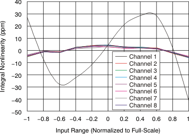
| Integral nonlinearity(5) | Full-scale with gain = 6, best fit | 8 | ppm | |||||
| Full-scale with gain = 6, best fit, ADS129xR channel 1 |
40 | ppm | ||||||
| –20 dBFS with gain = 6, best fit, ADS129xR channel 1 |
8 | ppm | ||||||
| Offset error | ±500 | µV | ||||||
| Offset error drift | 2 | µV/°C | ||||||
| Gain error | Excluding voltage reference error | ±0.2 | ±0.5 | % of FS | ||||
| Gain drift | Excluding voltage reference drift | 5 | ppm/°C | |||||
| Gain match between channels | 0.3 | % of FS | ||||||
| AC CHANNEL PERFORMANCE | ||||||||
| CMRR | Common-mode rejection ratio | fCM = 50 Hz, 60 Hz(2) | –105 | –115 | dB | |||
| PSRR | Power-supply rejection ratio | fPS = 50 Hz, 60 Hz | 90 | dB | ||||
| Crosstalk | fIN = 50 Hz, 60 Hz | –126 | dB | |||||
| SNR | Signal-to-noise ratio | fIN = 10 Hz input, gain = 6 | 112 | dB | ||||
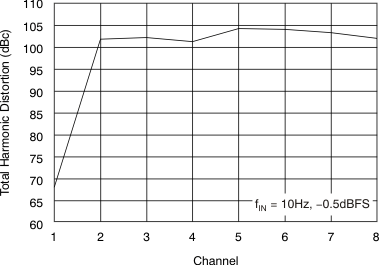
| THD | Total harmonic distortion(5) | 10 Hz, –0.5 dBFs | –98 | dB | ||||
| ADS129xR channel 1, 10 Hz, –0.5 dBFs | –70 | dB | ||||||
| 100 Hz, –0.5 dBFs(4) | –100 | dB | ||||||
| ADS129xR channel 1, 100 Hz, –0.5 dBFs(4) | –68 | dB | ||||||
| ADS129xR channel 1, 100 Hz, –20 dBFs(4) | –86 | dB | ||||||
| DIGITAL FILTER | ||||||||
| –3-dB bandwidth | 0.262 fDR | Hz | ||||||
| Digital filter settling | Full setting | 4 | Conversions | |||||
| RIGHT LEG DRIVE (RLD) AMPLIFIER AND PACE AMPLIFIERS | ||||||||
| RLD integrated noise | BW = 150 Hz | 7 | μVRMS | |||||
| Pace integrated noise | BW = 8 kHz | 20 | µVRMS | |||||
| Pace-amplifier crosstalk | Crosstalk between pace amplifiers | 60 | dB | |||||
| Gain bandwidth product | 50 kΩ || 10 pF load, gain = 1 | 100 | kHz | |||||
| Slew rate | 50 kΩ || 10 pF load, gain = 1 | 0.25 | V/μs | |||||
| Pace and RLD amplifier drive strength | Short circuit to GND (AVDD = 3 V) | 270 | μA | |||||
| Short circuit to supply (AVDD = 3 V) | 550 | μA | ||||||
| Short circuit to GND (AVDD = 5 V) | 490 | μA | ||||||
| Short circuit to supply (AVDD = 5 V) | 810 | μA | ||||||
| Pace and RLD current | Peak swing (AVSS + 0.3 V to AVDD + 0.3 V) at AVDD = 3 V |
50 | μA | |||||
| Peak swing (AVSS + 0.3 V to AVDD + 0.3 V) at AVDD = 5 V |
75 | μA | ||||||
| Pace-amplifier output resistance | 100 | Ω | ||||||
| Total harmonic distortion | fIN = 100 Hz, gain = 1 | –70 | dB | |||||
| Common-mode input range | AVSS + 0.7 | AVDD – 0.3 | V | |||||
| Common-mode resistor matching | Internal 200-kΩ resistor matching | 0.1% | ||||||
| Short-circuit current | ±0.25 | mA | ||||||
| Quiescent power consumption | Either RLD or pace amplifier | 20 | μA | |||||
| WILSON CENTRAL TERMINAL (WCT) AMPLIFIER | ||||||||
| Integrated noise | BW = 150 Hz | See Table 6 | nV/√Hz | |||||
| Gain bandwidth product | See Table 6 | kHz | ||||||
| Slew rate | See Table 6 | V/s | ||||||
| Total harmonic distortion | fIN = 100 Hz | 90 | dB | |||||
| Common-mode input range | AVSS + 0.3 | AVDD – 0.3 | V | |||||
| Short-circuit current | Through internal 30-kΩ resistor | ±0.25 | mA | |||||
| Quiescent power consumption | See Table 6 | μA | ||||||
| LEAD-OFF DETECT | ||||||||
| Frequency | See Table 16 for settings | 0, fDR/4 | kHz | |||||
| Current | See Table 16 for settings | 6, 12, 18, 24 | nA | |||||
| Current accuracy | ±20% | |||||||
| Comparator threshold accuracy | ±30 | mV | ||||||
| RESPIRATION (ADS129xR ONLY) | ||||||||
| Frequency | Internal source | 32, 64 | kHz | |||||
| External source | 32 | 64 | kHz | |||||
| Phase shift | See Table 16 for settings | 22.5 | 90 | 157.5 | Degrees | |||
| Impedance range | IRESP = 30 μA | 10 | kΩ | |||||
| Impedance measurement noise | 0.05-Hz to 2-Hz brick wall filter, 32-kHz modulation clock, phase = 112.5, IRESP = 30 μA with 2-kΩ baseline load, gain = 4 | 20 | mΩPP | |||||
| Modulator current | internal reference, signal path = 82 kΩ, baseline = 2.21 kΩ |
29 | µA | |||||
| EXTERNAL REFERENCE | ||||||||
| Input impedance | 10 | kΩ | ||||||
| INTERNAL REFERENCE | ||||||||
| Output voltage | Register bit CONFIG3.VREF_4V = 0, AVDD ≥ 2.7 V |
2.4 | V | |||||
| Register bit CONFIG3.VREF_4V = 1, AVDD ≥ 4.4 V |
4 | V | ||||||
| VREF accuracy | ±0.2% | |||||||
| Internal reference drift | TA = 25°C | 35 | ppm/°C | |||||
| Commercial grade, 0°C to 70°C | 35 | ppm | ||||||
| Industrial grade, –40°C to 85°C | 45 | ppm | ||||||
| Start-up time | 150 | ms | ||||||
| SYSTEM MONITORS | ||||||||
| Analog-supply reading error | 2% | |||||||
| Digital-supply reading error | 2% | |||||||
| Device wakeup | From power up to DRDY low | 150 | ms | |||||
| STANDBY mode | 9 | ms | ||||||
| Temperature-sensor reading, voltage | TA = 25°C | 145 | mV | |||||
| Temperature-sensor reading, coefficient | 490 | μV/°C | ||||||
| Test-signal frequency | See Table 16 for settings | fCLK / 221, fCLK / 220 | Hz | |||||
| Test-signal voltage | See Table 16 for settings | ±1, ±2 | mV | |||||
| Test-signal accuracy | ±2% | |||||||
| CLOCK | ||||||||
| Internal-oscillator clock frequency | Nominal frequency | 2.048 | MHz | |||||
| Internal clock accuracy | TA = 25°C | ±0.5% | ||||||
| 0°C ≤ TA ≤ 70°C | ±2% | |||||||
| –40°C ≤ TA ≤ 85°C, industrial grade versions only | ±2.5% | |||||||
| Internal-oscillator start-up time | 20 | μs | ||||||
| Internal-oscillator power consumption | 120 | μW | ||||||
| DIGITAL INPUT/OUTPUT (DVDD = 1.65 V to 3.6 V) | ||||||||
| VIH | High-level inpout voltage | 0.8 DVDD | DVDD + 0.1 | V | ||||
| VIL | Low-level input voltage | –0.1 | 0.2 DVDD | V | ||||
| VOH | High-level output voltage | IOH = –500 μA | DVDD – 0.4 | V | ||||
| VOL | Low-level output voltage | IOL = 500 μA | 0.4 | V | ||||
| IIN | Input current | 0 V < VDigitalInput < DVDD | –10 | 10 | μA | |||
| POWER SUPPLY (RLD, WCT, AND PACE AMPLIFIERS TURNED OFF) | ||||||||
| IAVDD | AVDD current | AVDD – AVSS = 3 V | HR mode (ADS1298) | 2.75 | mA | |||
| LP mode(6) (ADS1298) | 1.8 | mA | ||||||
| AVDD – AVSS = 5 V | HR mode (ADS1298) | 3.1 | mA | |||||
| LP mode (ADS1298) | 2.1 | mA | ||||||
| IDVDD | DVDD current | DVDD = 1.8 V | HR mode (ADS1298) | 0.3 | mA | |||
| LP mode (ADS1298) | 0.3 | mA | ||||||
| DVDD = 3 V | HR mode (ADS1298) | 0.5 | mA | |||||
| LP mode (ADS1298) | 0.5 | mA | ||||||
| Power dissipation | ADS1298, ADS1298R, AVDD – AVSS = 3 V | HR mode | 8.8 | 9.5 | mW | |||
| LP mode (250 SPS) | 6.0 | 7.0 | mW | |||||
| ADS1296, ADS1296R, AVDD – AVSS = 3 V | HR mode | 7.2 | 7.9 | mW | ||||
| LP mode (250 SPS) | 5.3 | 6.6 | mW | |||||
| ADS1294, ADS1294R, AVDD – AVSS = 3 V | HR mode | 5.4 | 6 | mW | ||||
| LP mode (250 SPS) | 4.1 | 4.4 | mW | |||||
| ADS1298, ADS1298R, AVDD – AVSS = 5 V | HR mode | 17.5 | mW | |||||
| LP mode (250 SPS) | 12.5 | mW | ||||||
| ADS1296, ADS1296R, AVDD – AVSS = 5 V | HR mode | 14.1 | mW | |||||
| LP mode (250 SPS) | 10 | mW | ||||||
| ADS1294, ADS1294R, AVDD – AVSS = 5 V | HR mode | 10.1 | mW | |||||
| LP mode (250 SPS) | 8.3 | mW | ||||||
| Power-down | AVDD – AVSS = 3 V | 10 | μW | |||||
| AVDD – AVSS = 5 V | 20 | μW | ||||||
| Standby mode | AVDD – AVSS = 3 V | 2 | mW | |||||
| AVDD – AVSS = 5 V | 4 | mW | ||||||
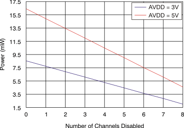
| Quiescent channel power | AVDD – AVSS = 3 V, PGA + ADC | 818 | μW | |||||
| AVDD – AVSS = 5 V, PGA + ADC | 1.5 | mW | ||||||
7.6 Timing Requirements: Serial Interface
specifications apply from TA = –40°C to +85°C (unless otherwise noted); load on DOUT = 20 pF || 100 kΩ| 2.7 V ≤ DVDD ≤ 3.6 V | 1.65 V ≤ DVDD ≤ 2 V | UNIT | ||||
|---|---|---|---|---|---|---|
| MIN | MAX | MIN | MAX | |||
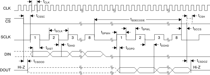
| tCLK | Master clock period | 414 | 514 | 414 | 514 | ns |
| tCSSC | CS low to first SCLK, setup time | 6 | 17 | ns | ||
| tSCLK | SCLK period | 50 | 66.6 | ns | ||
| tSPWH, L | SCLK pulse width, high and low | 15 | 25 | ns | ||
| tDIST | DIN valid to SCLK falling edge: setup time | 10 | 10 | ns | ||
| tDIHD | Valid DIN after SCLK falling edge: hold time | 10 | 11 | ns | ||
| tCSH | CS high pulse | 2 | 2 | tCLK | ||
| tSCCS | Eighth SCLK falling edge to CS high | 4 | 4 | tCLK | ||
| tSDECODE | Command decode time | 4 | 4 | tCLK | ||
| tDISCK2ST | DAISY_IN valid to SCLK rising edge: setup time | 10 | 10 | ns | ||
| tDISCK2HT | DAISY_IN valid after SCLK rising edge: hold time | 10 | 10 | ns | ||
7.7 Switching Characteristics: Serial Interface
specifications apply from TA = –40°C to +85°C (unless otherwise noted). Load on DOUT = 20 pF || 100 kΩ.| PARAMETER | 2.7 V ≤ DVDD ≤ 3.6 V | 1.65 V ≤ DVDD ≤ 2 V | UNIT | |||
|---|---|---|---|---|---|---|
| MIN | MAX | MIN | MAX | |||
| tDOHD | SCLK falling edge to invalid DOUT: hold time | 10 | 10 | ns | ||
| tDOPD | SCLK rising edge to DOUT valid: setup time | 17 | 32 | ns | ||
| tCSDOD | CS low to DOUT driven | 10 | 20 | ns | ||
| tCSDOZ | CS high to DOUT Hi-Z | 10 | 20 | ns | ||

7.8 Typical Characteristics
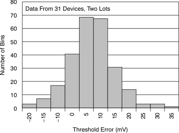
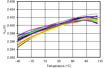
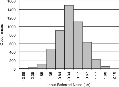
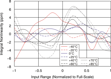
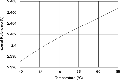
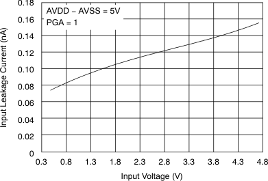
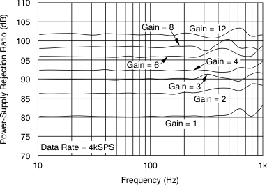
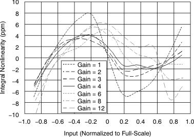
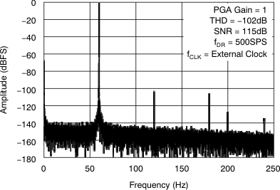
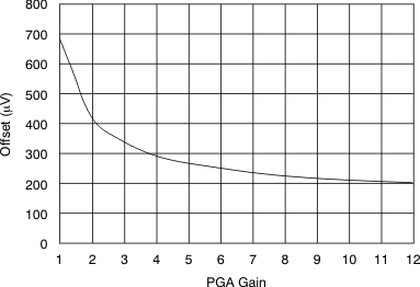
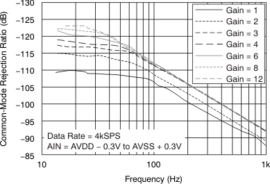
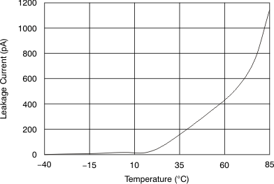
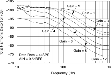
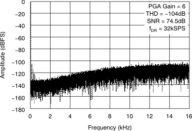
at TA = 25°C, AVDD = 3 V, AVSS = 0 V, DVDD = 1.8 V, internal VREFP = 2.4 V, VREFN = AVSS, external clock = 2.048 MHz, data rate = 500 SPS, high-resolution mode, and gain = 6 (unless otherwise noted)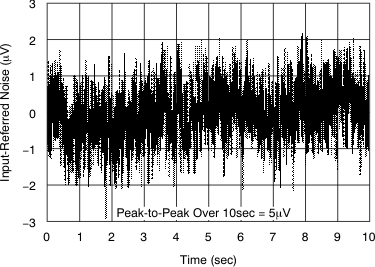
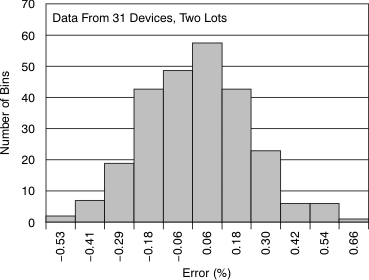
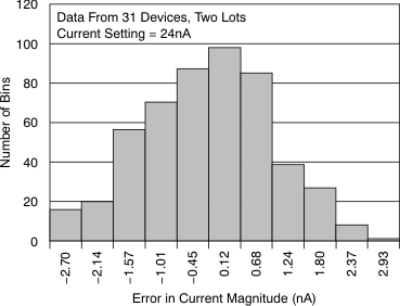
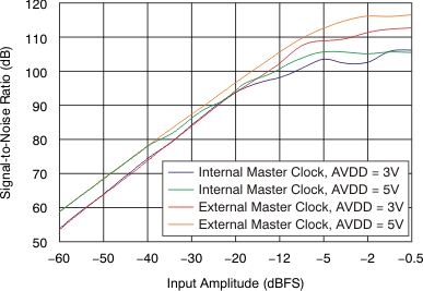
(10-Hz Sine Wave)
8 Parameter Measurement Information
8.1 Noise Measurements
NOTE
The ADS129xR channel performance differs from the ADS129x in regards to respiration circuitry found on channel one. Unless otherwise noted, ADS129x refers to all specifications and functional descriptions of the ADS1294, ADS1296, ADS1298, ADS1294R, ADS1296R, and ADS1298R. ADS129xR refers to all specifications and functional descriptions of only the ADS1294R, ADS1296R, and ADS1298R.
Optimize the ADS129x noise performance by adjusting the data rate and PGA setting. Reduce the data rate to increase the averaging, and the noise drops correspondingly. Increase the PGA value to reduce the input-referred noise. This lowered noise level is particularly useful when measuring low-level biopotential signals. Table 1 and Table 2 summarize the noise performance of the ADS129x in high-resolution (HR) mode and low-power (LP) mode, respectively, with a 3-V analog power supply. Table 3 and Table 4 summarize the noise performance of the ADS129x in HR and LP modes, respectively, with a 5-V analog power supply. The data are representative of typical noise performance at TA = 25°C. The data shown are the result of averaging the readings from multiple devices and are measured with the inputs shorted together. A minimum of 1000 consecutive readings are used to calculate the RMS and peak-to-peak noise for each reading. For the two highest data rates, the noise is limited by quantization noise of the ADC and does not have a gaussian distribution. Thus, the ratio between rms noise and peak-to-peak noise is approximately 10. For the lower data rates, the ratio is approximately 6.6.
Table 1 to Table 4 show measurements taken with an internal reference. The data are also representative of the ADS129x noise performance when using a low-noise external reference such as the REF5025.
Table 1. Input-Referred Noise μVRMS (μVPP) in High-Resolution Mode
3-V Analog Supply and 2.4-V Reference(1)
| DR BITS OF CONFIG1 REGISTER | OUTPUT DATA RATE (SPS) | –3-dB BANDWIDTH (Hz) | PGA GAIN = 1 |
PGA GAIN = 2 |
PGA GAIN = 3 |
PGA GAIN = 4 |
PGA GAIN = 6 |
PGA GAIN = 8 |
PGA GAIN = 12 |
|---|---|---|---|---|---|---|---|---|---|
| 000 | 32000 | 8398 | 335 (3553) | 168 (1701) | 112 (1100) | 85 (823) | 58 (529) | 42.5 (378) | 28.6 (248) |
| 001 | 16000 | 4193 | 56 (613) | 28 (295) | 18.8 (188) | 14.3 (143) | 9.7 (94) | 7.4 (69) | 5.2 (44.3) |
| 010 | 8000 | 2096 | 12.4 (111) | 6.5 (54) | 4.5 (37.9) | 3.5 (29.7) | 2.6 (21.7) | 2.2 (17.8) | 1.8 (13.8) |
| 011 | 4000 | 1048 | 6.1 (44.8) | 3.2 (23.3) | 2.4 (17.1) | 1.9 (14) | 1.5 (11.1) | 1.3 (9.7) | 1.2 (8.5) |
| 100 | 2000 | 524 | 4.1 (27.8) | 2.2 (15.4) | 1.6 (11) | 1.3 (9.1) | 1.1 (7.3) | 1 (6.5) | 0.9 (6) |
| 101 | 1000 | 262 | 2.9 (19) | 1.6 (10.1) | 1.2 (7.5) | 1 (6.2) | 0.8 (5) | 0.7 (4.6) | 0.6 (4.1) |
| 110 | 500 | 131 | 2.1 (12.5) | 1.1 (6.8) | 0.9 (5.1) | 0.7 (4.3) | 0.6 (3.5) | 0.5 (3.1) | 0.5 (2.9) |
Table 2. Input-Referred Noise μVRMS (μVPP) in Low-Power Mode
3-V Analog Supply and 2.4-V Reference(1)
| DR BITS OF CONFIG1 REGISTER | OUTPUT DATA RATE (SPS) | –3-dB BANDWIDTH (Hz) | PGA GAIN = 1 |
PGA GAIN = 2 |
PGA GAIN = 3 |
PGA GAIN = 4 |
PGA GAIN = 6 |
PGA GAIN = 8 |
PGA GAIN = 12 |
|---|---|---|---|---|---|---|---|---|---|
| 000 | 16000 | 4193 | 333 (3481) | 166 (1836) | 111 (1168) | 84 (834) | 56 (576) | 42 (450) | 28 (284) |
| 001 | 8000 | 2096 | 56 (554) | 28 (272) | 19 (177) | 14.3 (133) | 9.7 (85) | 7.4 (64) | 5 (42.4) |
| 010 | 4000 | 1048 | 12.5 (99) | 6.5 (51) | 4.5 (35) | 3.4 (25.9) | 2.4 (18.8) | 2 (14.5) | 1.5 (11.3) |
| 011 | 2000 | 524 | 6.1 (41.8) | 3.2 (22.2) | 2.3 (15.9) | 1.8 (12.1) | 1.4 (9.3) | 1.2 (7.8) | 1 (6.7) |
| 100 | 1000 | 262 | 4.1 (26.3) | 2.2 (14.6) | 1.6 (9.9) | 1.3 (8.1) | 1 (6.2) | 0.8 (5.4) | 0.7 (4.7) |
| 101 | 500 | 131 | 3 (17.9) | 1.6 (9.8) | 1.1 (6.8) | 0.9 (5.7) | 0.7 (4.2) | 0.6 (3.6) | 0.5 (3.4) |
| 110 | 250 | 65 | 2.1 (11.9) | 1.1 (6.3) | 0.8 (4.6) | 0.7 (4) | 0.5 (3) | 0.5 (2.6) | 0.4 (2.4) |
Table 3. Input-Referred Noise μVRMS (μVPP) in High-Resolution Mode
5-V Analog Supply and 4-V Reference(1)
| DR BITS OF CONFIG1 REGISTER | OUTPUT DATA RATE (SPS) | –3-dB BANDWIDTH (Hz) | PGA GAIN = 1 |
PGA GAIN = 2 |
PGA GAIN = 3 |
PGA GAIN = 4 |
PGA GAIN = 6 |
PGA GAIN = 8 |
PGA GAIN = 12 |
|---|---|---|---|---|---|---|---|---|---|
| 000 | 32000 | 8398 | 521 (5388) | 260 (2900) | 173 (1946) | 130 (1403) | 87 (917) | 65 (692) | 44 (483) |
| 001 | 16000 | 4193 | 86 (1252) | 43 (633) | 29 (402) | 22 (298) | 15 (206) | 11 (141) | 7 (91) |
| 010 | 8000 | 2096 | 17 (207) | 9 (112) | 6 (71) | 4 (57) | 3 (36) | 3 (29) | 2 (18) |
| 011 | 4000 | 1048 | 6.4 (48.2) | 3.4 (25.9) | 2.417.7) | 1.9 (15.4) | 1.5 (11.2) | 1.3 (9.6) | 1.1 (8.2) |
| 100 | 2000 | 524 | 4.2 (29.9) | 2.3 (15.9) | 1.6 (11.1) | 1.3 (9.3) | 1 (7.5) | 0.9 (6.6) | 0.8 (5.8) |
| 101 | 1000 | 262 | 2.9 (18.8) | 1.6 (10.4) | 1.1 (7.8) | 0.9 (6.1) | 0.7 (4.9) | 0.6 (4.7) | 0.6 (3.9) |
| 110 | 500 | 131 | 2 (12.8) | 1.1 (7.2) | 0.8 (5.2) | 0.7 (4) | 0.5 (3.3) | 0.5 (3.3) | 0.4 (2.7) |
Table 4. Input-Referred Noise μVRMS (μVPP) in Low-Power Mode
5-V Analog Supply and 4-V Reference(1)
| DR BITS OF CONFIG1 REGISTER | OUTPUT DATA RATE (SPS) | –3-dB BANDWIDTH (Hz) | PGA GAIN = 1 |
PGA GAIN = 2 |
PGA GAIN = 3 |
PGA GAIN = 4 |
PGA GAIN = 6 |
PGA GAIN = 8 |
PGA GAIN = 12 |
|---|---|---|---|---|---|---|---|---|---|
| 000 | 16000 | 4193 | 526 (5985) | 263 (2953) | 175 (1918) | 132 (1410) | 88 (896) | 66 (681) | 44 (458) |
| 001 | 8000 | 2096 | 88 (1201) | 44 (619) | 29 (411) | 22 (280) | 15 (191) | 11 (139) | 7 (83) |
| 010 | 4000 | 1048 | 17 (208) | 9 (103) | 6 (62) | 4 (52) | 3 (37) | 2 (25) | 2 (16) |
| 011 | 2000 | 524 | 6 (41.1) | 3.3 (23.3) | 2.2 (15.5) | 1.8 (12.3) | 1.3 (9.8) | 1.1 (7.8) | 0.9 (6.5) |
| 100 | 1000 | 262 | 4.1 (27.1) | 2.3 (14.8) | 1.5 (10.1) | 1.2 (8.1) | 0.9 (6) | 0.8 (5.4) | 0.7 (4.4) |
| 101 | 500 | 131 | 2.9 (17.4) | 1.6 (9.6) | 1.1 (6.6) | 0.9 (5.9) | 0.7 (4.3) | 0.6 (3.4) | 0.5 (3.2) |
| 110 | 250 | 65 | 2.1 (11.9) | 1.1 (6.6) | 0.8 (4.6) | 0.6 (3.7) | 0.5 (3) | 0.4 (2.5) | 0.4 (2.2) |

