SBAS895B May 2018 – April 2020
PRODUCTION DATA.
- 1 Features
- 2 Applications
- 3 Description
- 4 Revision History
- 5 Device Comparison Table
- 6 Pin Configuration and Functions
-
7 Specifications
- 7.1 Absolute Maximum Ratings
- 7.2 ESD Ratings
- 7.3 Recommended Operating Conditions
- 7.4 Thermal Information
- 7.5 Power Ratings
- 7.6 Insulation Specifications
- 7.7 Safety-Related Certifications
- 7.8 Safety Limiting Values
- 7.9 Electrical Characteristics
- 7.10 Switching Characteristics
- 7.11 Insulation Characteristics Curves
- 7.12 Typical Characteristics
- 8 Detailed Description
- 9 Application and Implementation
- 10Power Supply Recommendations
- 11Layout
- 12Device and Documentation Support
- 13Mechanical, Packaging, and Orderable Information
10 Power Supply Recommendations
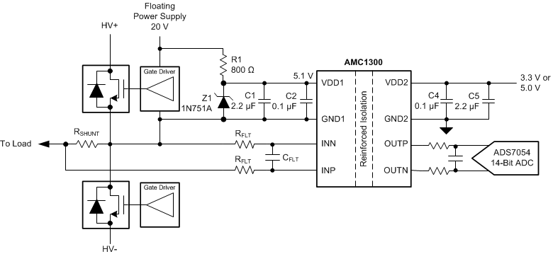
In a typical frequency inverter application, the high-side power supply (VDD1) for the device is directly derived from the floating power supply of the upper gate driver. For lowest system-level cost, a Zener diode can be used to limit the voltage to 5 V or 3.3 V (for the AMC1300B only) ± 10%. Alternatively, a low-cost low-dropout (LDO) regulator (for example, the LM317-N) may be used to minimize noise on the power supply. TI recommends a low-ESR decoupling capacitor of 0.1 µF to filter this power-supply path. Place this capacitor (C2 in Figure 55) as close as possible to the VDD1 pin of the AMC1300 for best performance. If better filtering is required, an additional 2.2-µF capacitor may be used. The floating ground reference (GND1) is derived from the end of the shunt resistor, which is connected to the negative input (INN) of the device. If a four-pin shunt is used, the device inputs are connected to the inner leads, and GND1 is connected to one of the outer leads of the shunt.
To decouple the low-side power supply on the controller side, use a 0.1-µF capacitor placed as close to the VDD2 pin of the AMC1300 as possible, followed by an additional capacitor from 1 µF to 10 µF.
 Figure 55. Zener-Diode-Based, High-Side Power Supply