SBAS895B May 2018 – April 2020
PRODUCTION DATA.
- 1 Features
- 2 Applications
- 3 Description
- 4 Revision History
- 5 Device Comparison Table
- 6 Pin Configuration and Functions
-
7 Specifications
- 7.1 Absolute Maximum Ratings
- 7.2 ESD Ratings
- 7.3 Recommended Operating Conditions
- 7.4 Thermal Information
- 7.5 Power Ratings
- 7.6 Insulation Specifications
- 7.7 Safety-Related Certifications
- 7.8 Safety Limiting Values
- 7.9 Electrical Characteristics
- 7.10 Switching Characteristics
- 7.11 Insulation Characteristics Curves
- 7.12 Typical Characteristics
- 8 Detailed Description
- 9 Application and Implementation
- 10Power Supply Recommendations
- 11Layout
- 12Device and Documentation Support
- 13Mechanical, Packaging, and Orderable Information
7.10 Switching Characteristics
over operating ambient temperature range (unless otherwise noted)| PARAMETER | TEST CONDITIONS | MIN | TYP | MAX | UNIT | |
|---|---|---|---|---|---|---|
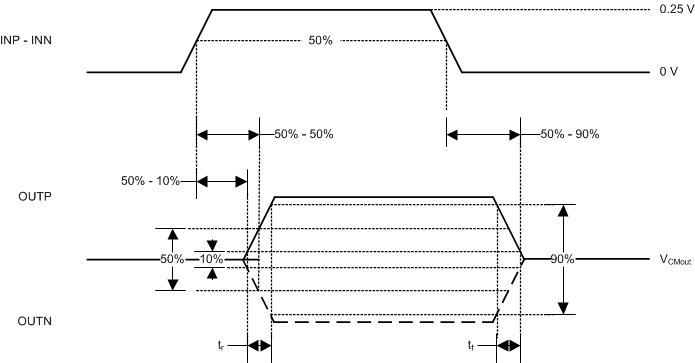
| tr | Rise time of OUTP, OUTN | See Figure 1 | 1.3 | µs | ||
| tf | Fall time of OUTP, OUTN | See Figure 1 | 1.3 | µs | ||
| INP, INN to OUTP, OUTN
signal delay (50% – 10%) |
AMC1300, unfiltered output, see Figure 1 | 1.5 | 2.2 | µs | ||
| INP, INN to OUTP, OUTN
signal delay (50% – 50%) |
1 | 1.5 | ||||
| INP, INN to OUTP, OUTN
signal delay (50% – 90%) |
AMC1300, unfiltered output, see Figure 1 | 2 | 2.7 | µs | ||
| AMC1300B, unfiltered output, see Figure 1 | 1.6 | 2.1 | ||||
| INP, INN to OUTP, OUTN
signal delay (50% – 90%) |
AMC1300, unfiltered output, see Figure 1 | 2.7 | 3.4 | µs | ||
| AMC1300B, unfiltered output, see Figure 1 | 2.5 | 3 | ||||
| tAS | Analog settling time | VDD1 step to 3.0 V with VDD2 ≥ 3.0 V,
to OUTP, OUTN valid, 0.1% settling |
500 | µs | ||
 Figure 1. Rise, Fall, and Delay Time Waveforms