SBAU193E June   2011  – May 2021 ADS8568


  1.   Trademarks
  2. 1EVM Overview
    1. 1.1 ADS8568EVM-PDK Kit Features
    2. 1.2 ADS8568EVM Board Features
    3. 1.3 Related Documentation From Texas Instruments
  3. 2EVM Analog Interface
    1. 2.1 ADC Supply, Input, Voltage Reference, and Digital Connections
    2. 2.2 ADC Amplifier Drive
  4. 3Digital Interface
    1. 3.1 Parallel Interface
    2. 3.2 Serial Interface (SPI)
    3. 3.3 Connections to PHI connector
    4. 3.4 Static Signals for ADS8568
    5. 3.5 I2C Bus for Onboard EEPROM
  5. 4Power Supplies
    1. 4.1 Low Dropout Regulator
    2. 4.2 Power Connections and LED Indicators
  6. 5Installing ADS8568EVM Software
  7. 6ADS8568EVM Operation
    1. 6.1 Connecting the Hardware and Running the GUI
    2. 6.2 Jumper Settings for ADS8568EVM
    3. 6.3 EVM GUI Global Settings for ADC Control
    4. 6.4 Time Domain Display
    5. 6.5 Frequency Domain Display
    6. 6.6 Histogram Display
  8. 7Modifying Hardware and Using Software to Evaluate ADS8548 and ADS8528
  9.   A Bill of Materials, Layout, and Schematic
    1.     A.1 Bill of Materials
    2.     A.2 Layout
    3.     A.3 Schematic
  10.   B Revision History

ADS8568EVM-PDK

GUID-20200707-SS0I-GRF1-517N-P3FKDWBZDBKG-low.gif

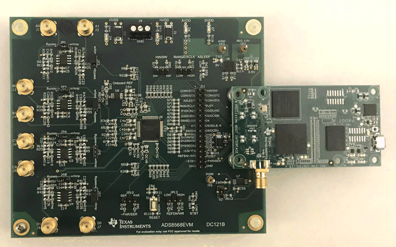
This user's guide describes the operation and use of the ADS8568 evaluation module (EVM). The ADS8568 is an 8-channel, simultaneous sampling, 16-bit successive approximation (SAR) analog-to-digital converter (ADC). Each input channel on the device can support true bipolar input ranges up to ±12 V. The device includes a programmable internal buffered voltage reverence. The ADC includes a serial SPI interface and a parallel interface for data communication. Configuration of the device is achieved through simple static digital input pins (hardware mode) or through communications to the SPI interface. This user's guide covers circuit description, schematic diagram, and bill of materials for the ADS8568 circuit board.