SBAU351 April   2021


  1.   Trademarks
  2. 1EVM Overview
    1. 1.1 ADS127L11EVM Kit
    2. 1.2 ADS127L11EVM Board
    3. 1.3 ADS127L11EVM-PDK-GUI Unsupported Features
  3. 2EVM Analog Interface
    1. 2.1 EVM Analog Input Options
    2. 2.2 ADC Connections and Decoupling
    3. 2.3 ADC Input Drive Amplifiers
    4. 2.4 VCOM Buffer
    5. 2.5 Onboard Voltage Reference
    6. 2.6 External Voltage Reference
    7. 2.7 Clock Tree
  4. 3Digital Interface
    1. 3.1 Serial Interface (SPI)
    2. 3.2 I2C Bus for Onboard EEPROM
  5. 4Power Supplies
    1. 4.1 Power Connection and Configuration
    2. 4.2 Low Dropout Regulator (LDO)
  6. 5ADS127L11EVM Software Installation
  7. 6EVM Operation
    1. 6.1 Connecting the Hardware
    2. 6.2 Optional Connections to the EVM
    3. 6.3 EVM GUI Global Settings for ADC Control
    4. 6.4 Time Domain Display
    5. 6.5 Frequency Domain Display
    6. 6.6 Histogram Display
  8. 7Bill of Materials, Schematics, and Layout
    1. 7.1 Bill of Materials
    2. 7.2 Board Layouts
    3. 7.3 Schematics
  9. 8References

I2C Bus for Onboard EEPROM

The circuit shown in Figure 3-2 is used with our EVM controller (PHI), for EVM identification. This circuit is not required by the ADS127L11 for operation. The jumper (JP1) is a write protect and does not need to be changed for EVM operation.
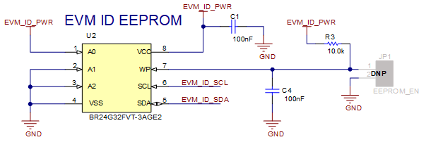
GUID-561974F8-9095-4948-8A2A-BC40780615A9-low.gifFigure 3-2 EEPROM for EVM ID