SBAU374A May 2021 – May 2022 DAC12DL3200
- Abstract
- Trademarks
- 1Introduction
- 2Equipment
-
3Setup Procedure
- 3.1 Install the High Speed Data Converter (HSDC) Pro Software
- 3.2 Install the Configuration GUI Software
- 3.3 Connect the DAC12DL3200EVM and TSW14DL3200EVM
- 3.4 Connect the Power Supplies to the Boards (Power Off)
- 3.5 Connect the Signal Generators to the EVM (*RF Outputs Disabled Until Directed)
- 3.6 Turn On the TSW14DL3200EVM 12-V Power and Connect to the PC
- 3.7 Turn On the DAC12DL3200EVM 5-V Power Supply and Connect to the PC
- 3.8 Turn On the Signal Generator RF Outputs
- 3.9 Open the DAC12DL3200EVM GUI and Program the DAC and Clocks for Single Channel, NRZ Mode 2 Operation
- 3.10 Open the HSDC Software and Load the FPGA Image to the TSW14DL3200EVM
- 3.11 DxSTRB Timing Adjustment
- 4Other Modes of Operation
- 5Register Log File
- 6Device Configuration
- A Troubleshooting the DAC12DL3200EVM
- B DAC12DL3200EVM Onboard Clocking Configuration
B DAC12DL3200EVM Onboard Clocking Configuration
This appendix provides settings for modifying the EVM for onboard clocking mode. In this mode, no external clocks are required. The LMK04828 uses the onboard 100-MHz VCXO and the internal PLL2 to provide the required clocks along with the LMX2592.
The DAC12DL3200EVM GUI provides 12 configuration files to be used with this mode. The following list describes a few of them:
- LMK_100M_LMX_6400M_Mode2_NRZ_Single_DAC.cfg: Operates the DAC in mode 2 with a sample rate of 6.4 GHz.
- LMK_100M_LMX_3200M_Mode0_NRZ_Dual_DAC.cfg: Operates the DAC in mode 0 with a sample rate of 3.2 GHz.
- LMK_100M_LMX_1600M_Mode1_NRZ_Dual_DAC.cfg: Operates the DAC in mode 1 with a sample rate of 1.6 GHz.
- LMK_100M_LMX_6400M_Mode0_2xRF_Dual_DAC.cfg: Operates the DAC in mode 0 with a sample rate of 6.4 GHz.
- LMK_100M_LMX_6400M_NCOA_1_4_100_400MHz.cfg: Operates the DAC in NCO mode with CHA output options of 100 MHz, 200 MHz, 300 MHz, and 400 MHz.
When using the "LMK_100M_LMX_6400M_Mode2_NRZ_Single_DAC.cfg" configuration file, the LMK04828 provides a 100-MHz reference clock to the LMX2592, a 50-MHz SYSREF clock to the DAC and a 400-MHz reference clock to the FPGA on the TSW14DL3200EVM.
The LMX2592 uses a 100-MHz reference clock from the LMK04828 and an internal PLL to provide the 6.4-GHz clock to the DAC. All clocks are synchronized to the 100-MHz VCXO.
To configure the DAC12DL3200EVM to use onboard clock mode, complete the following steps:
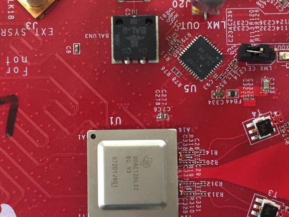
- Remove C7 and C6, and populate C277 and C278.
- Install FB28 with MuRata BLM18AG121TN1D or equivalent. This is located on the bottom of the board under Y2.
- Remove the shunt on the LMX_CE
jumper J6.
 Figure B-1 Onboard Clocking
Setup
 - Remove the signal generators.
- Program the DAC using the
DAC12DL3200 GUI.
- Press the DAC RESET switch on the EVM.
- In the DAC GUI Low Level View tab, select the configuration file called "LMK_100M_LMX_6400M_Mode2_NRZ_Single_DAC.cfg".
- Send a test pattern using HSDC Pro GUI.
The LMK04828 routes a spare clock (DCLK10) to SMBs J26 and J28 that can be used to verify LMK operation. By default, the GUI has this clock disabled. Use the LMK04828 Clock Outputs tab to enable this clock. Set CLKout 10 and 11 DCLK Type to "LVPECL 2000 mV" and DCLK Divider to "24" to provide a 100-MHz clock to these SMBs (LMKOUTP, LMKOUTN).
The LMX2592 routes a spare clock (RFOUTB) to SMB J20 that can be used to verify LMX operation. By default, the GUI has this clock disabled. Click on the LMX2592 tab and uncheck the OUTB PD box. There is now a 6.4-GHz tone on SMB connector J20 (LMX OUT).
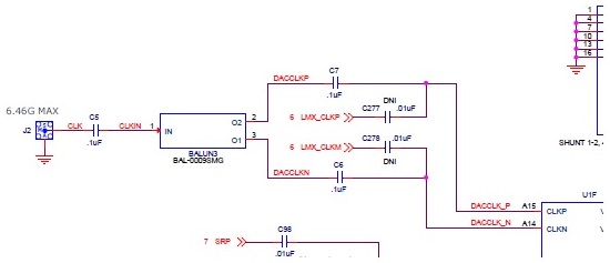
 Figure B-2 Default Board Clock
Configuration Circuit (External Clock Mode)
Figure B-2 Default Board Clock
Configuration Circuit (External Clock Mode)The LMX2582 and LMK04828 may be reconfigured to exercise more features, but this EVM is not intended to be a full evaluation platform for these devices. For a full evaluation platform, see the LMK04828EVM tool folder and LMX2592EVM tool folder.