SBAU446 December 2023 ADC3683-SP
1.3 Specification
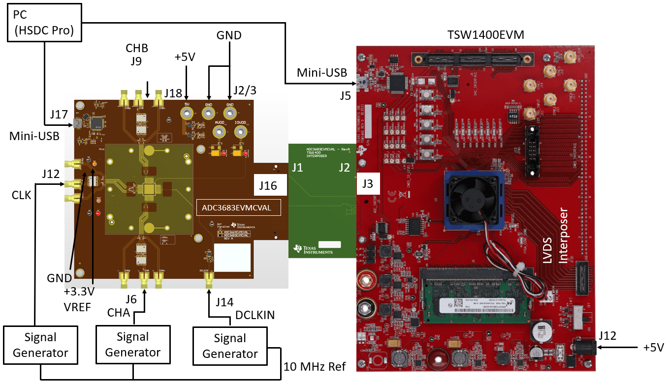
The ADC36xxEVMCVAL receives power from the 5 V jack at J18, which is then converted to +1.8 VDC for AVDD and +1.8 VDC for DVDD. This conversion happens by way of two ultra-low noise, ultra-high PSRR, low-dropout regulators, TPS7A9401DSC. USB-to-SPI communication is established using the FTDI (FT4232HL-REEL). The ADC clocks are supplied externally. The default configuration is to input the device clock (CLK) single-ended into J12 and the data clock (DCLK) single-ended into J14 (high quality external clocks are used to achieve best AC performance). The analog inputs by default are supplied through J6 for channel A and J9 for channel B where the signal is AC coupled through the baluns (ADT4-1WT). The analog input full-scale is 3.2 Vpp. The analog input is driven at -1 dBFs (approximately 2.8 Vpp) in all examples in this user's guide.
The ADC36XXQML-SP family has a +1.6 V voltage reference (VREF) that can be supplied internally or externally. By default, the EVM is configured to supply an external voltage reference using REF35160QDBVR Precision Voltage Reference which is supplied using the VREF test point and 3.3 V supply. At any time, the reference can be changed to internal via SPI write.
The ADC36XXQML-SP family uses an unbuffered analog input, so a glitch filter is required to attenuate the ADC sampling glitch from when the sampling capacitors switch (sample/hold). The glitch filter acts as a low pass filter with a corner frequency (Fc) at 30 MHz (accepts DC to 30 MHz).
The ADC36xxEVMCVAL LVDS output data is routed to an FMC connector, and then connected to an LVDS Interposer card. This interposer card then maps to the HSMC connector of the TSW1400EVM to capture the ADC36xxEVMCVAL SLVDS clock and data signals.
 Figure 1-1 ADC36xxEVMCVAL Block Diagram