SBAU446 December 2023 ADC3683-SP
3.5 Setup
Before setup, make sure the necessary software is downloaded and installed, as described in Section 2. Go ahead and open HSDC Pro and ADC35XX EVM GUI.
As an additional note, there are not any jumpers or headers that need to be checked or addressed.
First, connect the FMC data interface of the ADC36xxEVMCVAL (J16) to J1 of the LVDS interposer card (ADC3683_TSW1400_Interposer_RevA). Then, connect the HSMC interface of the LVDS interposer card to J3 of the TSW1400EVM.
Connect one mini-USB cable to the TSW1400EVM (J5) and another mini-USB cable to the ADC36xxEVMCVAL (J17).
Connect 5 V (4 A capable supply) to J12 of the TSW1400EVM. Turn the TSW1400EVM on using SW7.
Connect 5 V (1 A capable supply) banana jack to J18 of the ADC36xxEVMCVAL and the corresponding ground banana jack to J2 or J3 of the EVM. Turn the power supply on.
Connect 3.3 V (1 A capable supply) via a clip to VREF test point on the ADC36xxEVMCVAL and the corresponding ground clip to the most convenient GND test point on the EVM. Turn the power supply on.
Using a multi-meter, set the measure to volts (DC) and verify the following test points have the following voltage levels on the ADC36xxEVMCVAL.
| Test Point | Voltage (V) |
|---|---|
| IOVDD | +1.8 VDC +/- 0.1 V |
| AVDD | +1.8 VDC +/- 0.1 V |
| VREF | +3.3 VDC +/- 0.1 V |
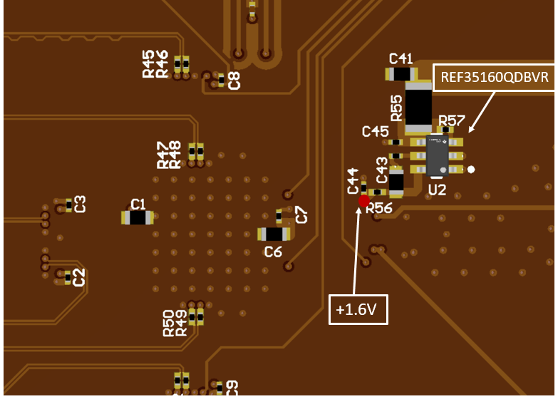
Also using the multi-meter and the same settings above, verify the voltage at the node between R56 and C44 (bottom side of the board) is +1.6 VDC +/- 0.1 V. This is the voltage to be supplied as the external reference to the part. See the images below for reference to this location.
 Figure 3-5 VREF (+1.6 V) Node
 Figure 3-6 VREF Schematic
Connect an SMA cable between the output of a signal generator and the input of a 5 MHz band-pass filter. Set the frequency of the signal generator to 5 MHz with an amplitude of +10 dBm. Then connect an SMA cable between the output of the 5 MHz band-pass filter and the analog input of the ADC36xxEVMCVAL (J6) for Channel A. For Channel B testing, connect to J9. This is the analog input.
Connect an SMA cable between the output of a signal generator and the input of a 65 MHz band-pass filter. Set the frequency of the signal generator to 65 MHz with an amplitude of +10 dBm. Then connect an SMA cable between the output of the 65 MHz filter and the CLK input of the ADC36xxEVMCVAL (J12). The is the device sampling clock.
Connect an SMA cable to the output of a signal generator and the input of DCLKIN (J14) of the ADC36xxEVMCVAL. Set the frequency of the signal generator to 292.5 MHz with an amplitude of 0 dBm.
One important point is that the signal generators referenced above must share the same reference frequency (frequency locked). This is usually accomplished by connecting the 10 MHz input and output ports on the back panel of the signal generators using BNC cables.