SBAU452 March   2024


  1.   1
  2.   Description
  3.   Features
  4.   4
  5. 1Evaluation Module Overview
    1.     6
    2. 1.1 Introduction
    3. 1.2 Kit Contents
    4. 1.3 Specification
    5. 1.4 Device Information
    6. 1.5 General Texas Instruments High Voltage Evaluation (TI HV EVM) User Safety Guidelines
  6. 2Hardware
    1. 2.1 Circuitry
      1. 2.1.1 Pin Headers and Test Points
      2. 2.1.2 Bypass Capacitors
      3. 2.1.3 Load Connectors
      4. 2.1.4 TMCS Isolated Current-Sense Amplifier
    2. 2.2 Board Assembly
    3. 2.3 Measurements
      1. 2.3.1 Input Connection
      2. 2.3.2 Advanced Measurement Tips
  7. 3Hardware Design Files
    1. 3.1 Schematics
    2. 3.2 PCB Layout
    3. 3.3 Bill of Materials
  8. 4Additional Information
    1. 4.1 Trademarks
  9. 5Related Documentation From Texas Instruments

PCB Layout

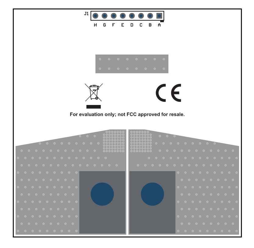
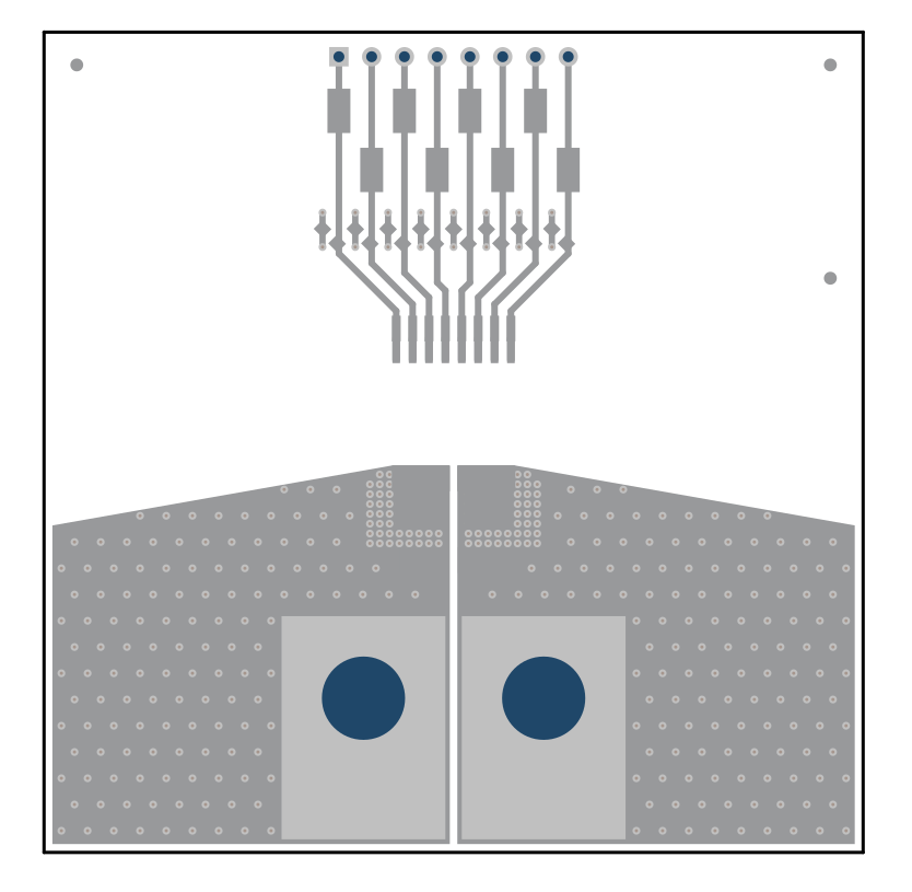
Figure 4-2 through Figure 4-7 illustrate the PCB layers of the TMCS-A-ADAPTER-EVM.

Note: Board layouts are not to scale. These figures are intended to show how the board is laid out. The figures are not intended to be used for manufacturing TMCS-A-ADAPTER-EVM PCBs.
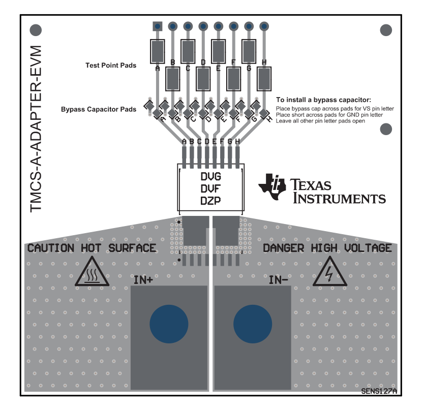
GUID-20240320-SS0I-HXR4-M9W7-LTWGPWBKR2HH-low.png Figure 3-2 Top Overlay
GUID-20240320-SS0I-DXQW-G088-KNRZZ47L9KK3-low.png Figure 3-3 Bottom Overlay
GUID-20240320-SS0I-NBBF-ZN13-FFGB8QCN1RXL-low.png Figure 3-4 Top Layer
GUID-20240320-SS0I-5WQX-KCK6-FHQF57XSHKXZ-low.png Figure 3-5 Copper Layer 1
GUID-20240320-SS0I-FF5M-D8TV-WD5SQ3BHCZGP-low.png Figure 3-6 Copper Layer 2
GUID-20240320-SS0I-SKFV-VQXC-LJCCF2VBZ2WW-low.png Figure 3-7 Bottom Layer