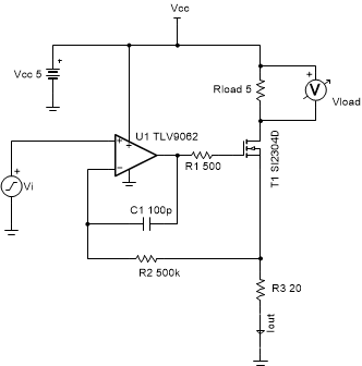
Voltage-to-current (V-I) converter circuit with MOSFET
Design Goals
| Input | Output | Supply | |||
|---|---|---|---|---|---|
| ViMin | ViMax | IoMin | IoMax | Vcc | Vee |
| 0V | 2V | 0mA | 100mA | 5V | 0V |
Design Description
This single-supply, low-side, V-I converter delivers a well-regulated current to a load which can be connected to a voltage greater than the op-amp supply voltage. The circuit accepts an input voltage between 0V and 2V and converts it to a current between 0mA and 100mA. The current is accurately regulated by feeding back the voltage drop across a low-side current-sense resistor, R3, to the inverting input of the op amp.
Design Notes
- A device with a rail-to-rail input (RRI) or common-mode voltage that extends to GND is required.
- R1 helps isolate the amplifier from the capacitive load of the MOSFET gate.
- Feedback components R2 and C1 provide compensation to ensure stability during input or load transients, which also helps reduce noise. R2 provides a DC feedback path directly at the current setting resistor (R3) and C1 provides a high-frequency feedback path that bypasses the MOSFET.
- The input bias current will flow through R2, which will cause a DC error. Therefore, ensure that this error is minimal compared to the offset voltage of the op amp.
- Use the op amp in a linear operating region. Linear output swing is usually specified under the AOL test conditions provided in the op amp data sheet.
Design Steps
- Determine the transfer function.
- Calculate the sense resistor, R3.
- Calculate the maximum power dissipated into the sense resistor, R3, to ensure the resistor power ratings are not exceeded.
- See the Design References section, [2] for the design procedure on how to properly size the compensation components, R1, R2, and C1.
Design Simulations
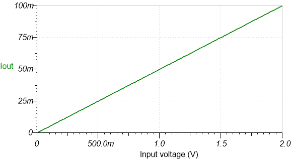
DC Simulation Results
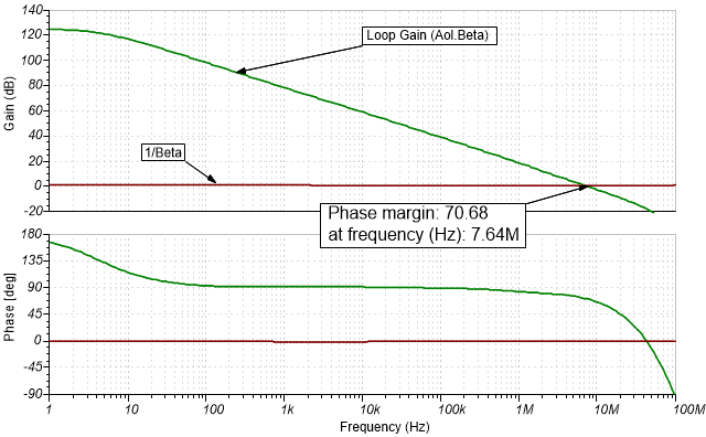
Loop Stability Simulation Results
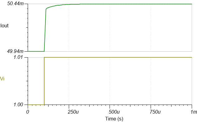
Step Response
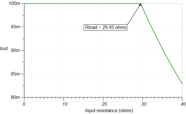
Compliance Voltage
Set output to full-scale (100 mA) and test the maximum load resistance.
Design References
- See Analog Engineer's Circuit Cookbooks for TI's comprehensive circuit library.
- TI Precision Labs
Design Featured Op Amp
| TLV9062 | |
|---|---|
| Vss | 1.8 V to 5.5 V |
| VinCM | Rail-to-rail |
| Vout | (Vcc + 60mV) to (Vee – 60mV) at RL = 2kΩ |
| Vos | 1.6mV |
| Iq | 0.538mA |
| Ib | 0.5pA |
| UGBW | 10MHz |
| SR | 6.5V/µs |
| #Channels | 1, 2, 4 |
| www.ti.com/product/TLV9062 | |
Design Alternate Op Amp
| TLV9042 |
OPA2182 |
|
|---|---|---|
| Vss | 1.2V to 5.5V |
4.5V to 36V |
| VinCM | Rail-to-rail |
(Vee – 0.1V) to (Vcc – 2.5V) |
| Vout | Rail-to-rail |
Rail-to-rail |
| Vos | ±0.6mV |
±0.45μV |
| Iq |
0.01mA |
0.85mA |
| Ib | ±1pA |
±50pA |
| UGBW | 350kHz |
5MHz |
| SR | 0.2V/µs |
10V/μS |
| #Channels |
1,2,4 |
2 |
| www.ti.com/product/TLV9042 |
IMPORTANT NOTICE AND DISCLAIMER
| TI PROVIDES TECHNICAL AND RELIABILITY DATA (INCLUDING DATASHEETS), DESIGN RESOURCES (INCLUDING REFERENCE DESIGNS), APPLICATION OR OTHER DESIGN ADVICE, WEB TOOLS, SAFETY INFORMATION, AND OTHER RESOURCES “AS IS” AND WITH ALL FAULTS, AND DISCLAIMS ALL WARRANTIES, EXPRESS AND IMPLIED, INCLUDING WITHOUT LIMITATION ANY IMPLIED WARRANTIES OF MERCHANTABILITY, FITNESS FOR A PARTICULAR PURPOSE OR NON-INFRINGEMENT OF THIRD PARTY INTELLECTUAL PROPERTY RIGHTS. |
| These resources are intended for skilled developers designing with TI products. You are solely responsible for (1) selecting the appropriate TI products for your application, (2) designing, validating and testing your application, and (3) ensuring your application meets applicable standards, and any other safety, security, or other requirements. These resources are subject to change without notice. TI grants you permission to use these resources only for development of an application that uses the TI products described in the resource. Other reproduction and display of these resources is prohibited. No license is granted to any other TI intellectual property right or to any third party intellectual property right. TI disclaims responsibility for, and you will fully indemnify TI and its representatives against, any claims, damages, costs, losses, and liabilities arising out of your use of these resources. |
| TI’s products are provided subject to TI’s Terms of Sale (www.ti.com/legal/termsofsale.html) or other applicable terms available either on ti.com or provided in conjunction with such TI products. TI’s provision of these resources does not expand or otherwise alter TI’s applicable warranties or warranty disclaimers for TI products. |
| Mailing Address: Texas Instruments, Post Office Box 655303, Dallas, Texas 75265
Copyright © 2021, Texas Instruments Incorporated |