SBOS853B March 2017 – December 2024
PRODUCTION DATA
- 1
- 1 Features
- 2 Applications
- 3 Description
- 4 Pin Configuration and Functions
- 5 Specifications
- 6 Detailed Description
-
7 Register Maps
- 7.1
Internal Registers
- 7.1.1
Register Descriptions
- 7.1.1.1 Result Register (offset = 00h)
- 7.1.1.2 Configuration Register (offset = 01h) [reset = C810h]
- 7.1.1.3 Low-Limit Register (offset = 02h) [reset = C0000h]
- 7.1.1.4 High-Limit Register (offset = 03h) [reset = BFFFh]
- 7.1.1.5 Manufacturer ID Register (offset = 7Eh) [reset = 5449h]
- 7.1.1.6 Device ID Register (offset = 7Fh) [reset = 3001h]
- 7.1.1
Register Descriptions
- 7.1
Internal Registers
- 8 Application and Implementation
- 9 Device and Documentation Support
- 10Revision History
- 11Mechanical, Packaging, and Orderable Information
8.2.2.2 Dark Window Selection and Compensation
There are several approaches to selecting and compensating for a dark window. One of many approaches is the method described in this section.
Sample several different windows with various levels of darkness. Choose a window that is dark enough to optimize the balance between the aesthetics of the device and sensor performance. Note that the aesthetic evaluation is the subjective opinion of the designer; observing the window on the physical design is preferred over referring to the window transmission specifications. Verify that the selected window is not darker than absolutely necessary because a darker window allows less light to illuminate the sensor and therefore impedes sensor accuracy.
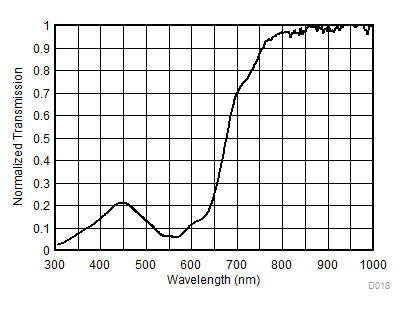
The window chosen for this application example is dark and has less than 7% transmission at 550nm. Figure 8-3 shows the normalized response of the spectrum. Note that the equipment used to measure the transmission spectrum is not capable of measuring the absolute accuracy (non-normalized) of the dark window sample, but only the relative normalized spectrum. Also note that the window is much more transmissive to infrared wavelengths longer than 700nm than to visible wavelengths between 400nm and 650nm. This imbalance between infrared and visible light decreases the ratio of visible light to infrared light at the sensor. Although having the window decrease this ratio as little as possible (by having a window with a close ratio of visible transmission to infrared transmission) is preferred, the OPT3001-Q1 device still performs well as shown in Figure 8-6.
 Figure 8-3 Normalized Transmission Spectral Response of the Chosen Dark Window
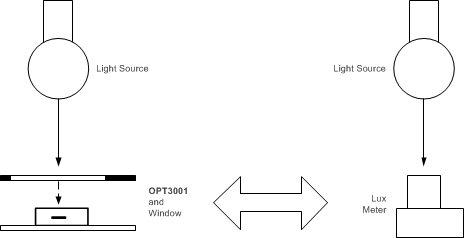
After choosing the dark window, measure the attenuating effect of the dark window for later compensation. To measure this attenuation, measure a fluorescent light source with a lux meter, then measure that same light with the OPT3001-Q1 device under the dark window. To measure accurately, use a fixture that can accommodate either the lux meter or the design containing the OPT3001-Q1 device and dark window, with the center of each of the sensing areas being in exactly the same X, Y, Z location, as shown in Figure 8-4. The Z placement of the design (distance from the light source) is the top of the window, and not the OPT3001-Q1 device.
 Figure 8-4 Fixture With One Light Source Accommodating Either a Lux Meter or the Design (Window and OPT3001-Q1 Device) in the Exact Same X,Y,Z Position
The fluorescent light in this location measures 1000lux with the lux meter, and 73lux with the OPT3001-Q1 device under the dark window within the application. Therefore, the window has an effective transmission of 7.3% for the fluorescent light. This 7.3% is the weighted average attenuation across the entire spectrum, weighted by the spectral response of the lux meter (or photopic response).
For all subsequent OPT3001-Q1 measurements under this dark window, the following formula is applied.