SBOSA30D March   2022  – December 2024

PRODUCTION DATA  

  1.   1
  2. Features
  3. Applications
  4. Description
  5. Device Comparison
  6. Pin Configuration and Functions
  7. Specifications
    1. 6.1 Absolute Maximum Ratings
    2. 6.2 ESD Ratings
    3. 6.3 Recommended Operating Conditions
    4. 6.4 Thermal Information
    5. 6.5 Electrical Characteristics
    6. 6.6 Typical Characteristics
  8. Detailed Description
    1. 7.1 Overview
    2. 7.2 Functional Block Diagram
    3. 7.3 Feature Description
      1. 7.3.1 Amplifier Input Common-Mode Signal
        1. 7.3.1.1 Enhanced PWM Rejection Operation
        2. 7.3.1.2 Input-Signal Bandwidth
        3. 7.3.1.3 Low Input Bias Current
        4. 7.3.1.4 Low VSENSE Operation
        5. 7.3.1.5 Wide Fixed Gain Output
        6. 7.3.1.6 Wide Supply Range
    4. 7.4 Device Functional Modes
      1. 7.4.1 Adjusting the Output With the Reference Pins
      2. 7.4.2 Reference Pin Connections for Unidirectional Current Measurements
        1. 7.4.2.1 Ground Referenced Output
        2. 7.4.2.2 VS Referenced Output
      3. 7.4.3 Reference Pin Connections for Bidirectional Current Measurements
        1. 7.4.3.1 Output Set to External Reference Voltage
        2. 7.4.3.2 Output Set to Mid-Supply Voltage
        3. 7.4.3.3 Output Set to Mid-External Reference
        4. 7.4.3.4 Output Set Using Resistor Divider
      4. 7.4.4 High Signal Throughput
  9. Application and Implementation
    1. 8.1 Application Information
      1. 8.1.1 RSENSE and Device Gain Selection
    2. 8.2 Typical Application
      1. 8.2.1 Inline Motor Current-Sense Application
        1. 8.2.1.1 Design Requirements
        2. 8.2.1.2 Detailed Design Procedure
        3. 8.2.1.3 Application Curve
    3. 8.3 Power Supply Recommendations
      1. 8.3.1 Power Supply Decoupling
    4. 8.4 Layout
      1. 8.4.1 Layout Guidelines
      2. 8.4.2 Layout Examples
  10. Device and Documentation Support
    1. 9.1 Documentation Support
      1. 9.1.1 Related Documentation
    2. 9.2 Receiving Notification of Documentation Updates
    3. 9.3 Support Resources
    4. 9.4 Trademarks
    5. 9.5 Electrostatic Discharge Caution
    6. 9.6 Glossary
  11. 10Revision History
  12. 11Mechanical, Packaging, and Orderable Information

Adjusting the Output With the Reference Pins

Figure 7-2 shows a test circuit for reference-divider accuracy. The INA241x output is configurable to allow for unidirectional or bidirectional operation.
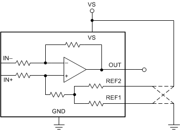
INA241A INA241B Test Circuit For Reference Divider AccuracyFigure 7-2 Test Circuit For Reference Divider Accuracy

The output voltage is set by applying a voltage or voltages to the reference voltage inputs, REF1 and REF2. The reference inputs are connected to an internal gain network. There is no operational difference between the two reference pins. The resistor network connected to the two reference pins are designed with ultra-precision and matching. Output is set accurately at the mid-point voltage between the voltages applied to reference voltage inputs, when current-sense input voltage is 0V as shown in Equation 1. In most bidirectional applications, one reference input is connected to the positive supply and the other reference input is connected to the negative supply (GND pin) to set the output voltage to mid-supply.

Equation 1. V O U T = G × V I N + -   V I N - + V R E F 1 +   V R E F 2 2