SBOU024C august 2004 – july 2023 PGA309
- 1
- Read This First
-
1Introduction
- 1.1 PGA309 Functional Description
- 1.2 Sensor Error Adjustment Range
- 1.3 Gain Scaling
- 1.4 Offset Adjustment
- 1.5 Voltage Reference
- 1.6 Sensor Excitation and Linearization
- 1.7 ADC for Temperature Sensing
- 1.8 External EEPROM and Temperature Coefficients
- 1.9 Fault Monitor
- 1.10 Over-Scale and Under-Scale Limits
- 1.11 Power-Up and Normal Operation
- 1.12 Digital Interface
- 1.13 Pin Configuration
- 2Detailed Description
- 3Operating Modes
-
4Digital Interface
- 4.1 Description
- 4.2 Two-Wire Interface
- 4.3 One-Wire Interface
- 4.4 One-Wire Interface Timeout
- 4.5 One-Wire Interface Timing Considerations
- 4.6 Two-Wire Access to External EEPROM
- 4.7 One-Wire Interface Initiated Two-Wire EEPROM Transactions
- 4.8 PGA309 Stand-Alone Mode and Two-Wire Transactions
- 4.9 PGA309 Two-Wire Bus Master Operation and Bus Sharing Considerations
- 4.10 One-Wire Operation with PRG Connected to VOUT
- 4.11 Four-Wire Modules and One-Wire Interface (PRG)
- 5Application Background
-
6Register Descriptions
- 6.1 Internal Register Overview
- 6.2
Internal Register Map
- 6.2.1 Register 0: Temp ADC Output Register (Read Only, Address Pointer = 00000)
- 6.2.2 Register 1: Fine Offset Adjust (Zero DAC) Register (Read/Write, Address Pointer = 00001)
- 6.2.3 Register 2: Fine Gain Adjust (Gain DAC) Register (Read/Write, Address Pointer = 00010)
- 6.2.4 Register 3: Reference Control and Linearization Register (Read/Write, Address Pointer = 00011)
- 6.2.5 Register 4: PGA Coarse Offset Adjust and Gain Select/Output Amplifier Gain Select Register (Read/Write, Address Pointer = 00100)
- 6.2.6 Register 5: PGA Configuration and Over/Under-Scale Limit Register (Read/Write, Address Pointer = 00101)
- 6.2.7 Register 6: Temp ADC Control Register (Read/Write, Address Pointer = 00110)
- 6.2.8 Register 7: Output Enable Counter Control Register (Read/Write, Address Pointer = 00111)
- 6.2.9 Register 8: Alarm Status Register (Read Only, Address Pointer = 01000)
- A External EEPROM Example
- B Detailed Block Diagram
- C Glossary
- Revision History
2.7.1 Temp ADC Start-Convert Control
The Temp ADC has two conversion modes: Single and Continuous. In Continuous Conversion mode (CEN = ‘1’), the Temp ADC initiates the next conversion cycle immediately after a conversion is complete. In Single Conversion mode (CEN = ‘0’) the Temp ADC start-convert bit (ADCS) acts as a start-convert/busy bit and must be set to ‘1’ before a conversion is initiated. Setting ADCS to ‘1’ occurs when the register configuration section of the EEPROM (part one) contains ADCS = ‘1’ and the EEPROM is read. Furthermore, ADCS will be reset to ‘1’ for each successive EEPROM read. After ADCS is set to ‘1’, it will be a ‘1’ if read immediately and can be polled until it returns to a ‘0’, indicating the conversion is complete. The Start-Convert modes are shown in Table 2-13.
| CEN [10] | ADCS [12] | Conversion Mode | Comments |
|---|---|---|---|
| 0 | 0 | Single | Temp ADC mode—no conversions. |
| 0 | 1 | Single | Temp ADC starts conversion and ADCS acts as busy bit with it changing to a '0' at end of conversion. |
| 1 | X | Continuous | ADCS bit exercises no control—typically ADCS = '1' since conversions are continuous |
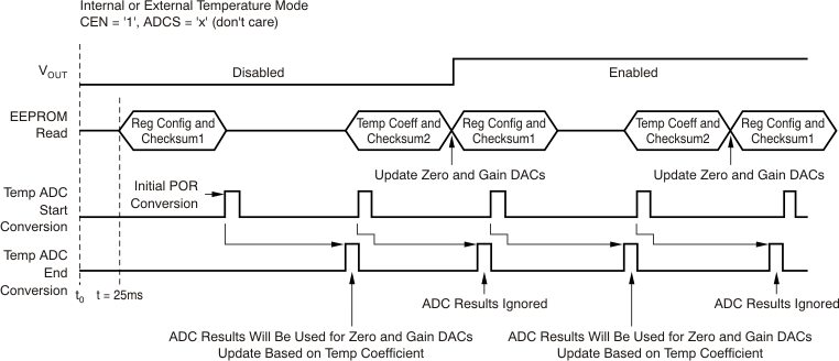
In Figure 2-18 continuous start-convert control is selected. After an initial power-on reset timeout of typically 33ms, the register configuration section of the EEPROM (part one) is read. Immediately after this, a Temp ADC conversion is started. At the end of this first conversion, the temperature coefficients section of the EEPROM (part two) are read, and Zero and Gain DAC settings are adjusted. Since CEN = ‘1’, the end of each conversion will start the next conversion. After the temperature coefficients section of the EEPROM (part two) has been read, the register configuration values are read. Note that reading of the second half of the EEPROM (temperature coefficients) is triggered by a valid register configuration read of the EEPROM. This operation yields the most temperature updates over a given time period.
 Figure 2-18 Temp ADC Continuous Start-Convert Control
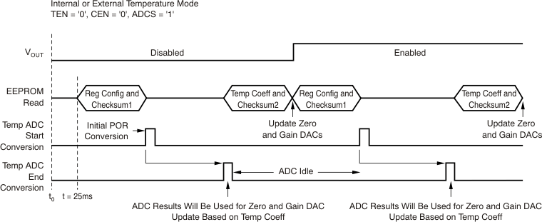
In Figure 2-19, Single Conversion mode is selected (CEN = ‘0’). After an initial power-on reset timeout of typically 33ms, the register configuration (part one) of the EEPROM is read. Immediately after this, a Temp ADC conversion is started if CEN = ‘0’ and ADCS = ‘1’. At the end of this first conversion, the temperature coefficients (part two) of the EEPROM are read, and Zero and Gain DAC settings are adjusted. When CEN = ‘0’ and ADCS = ‘1’, a new start conversion occurs only after reading the register configuration part of the EEPROM. At the end of this conversion, the second part of the EEPROM (temperature coefficients) is read, the Gain and Zero DAC temperature calculations are done, and each respective DAC updated. Note that in the Single Start-Convert mode, if CEN = ‘0’ and ADCS = ‘0’ (no Temp ADC conversions), the PGA309 will wait 33ms after power-on, read the register configuration part of the EEPROM, and without an ADC conversion, read the Lookup Table and calculate Gain and Zero DAC values. These values are based on the current ADC output register (all zero on power-up). The PGA309 output will then be enabled and will wait about 25ms, and read the register configuration part of the EEPROM. The output remains enabled with a continuous loop of reading the register configuration part of the EEPROM, waiting 33ms, and read again.
One final control option for External Temperature Mode is the ADC2X bit, Register 6 bit [13]. This bit allows the conversion speed of the Temp ADC to be increased for external temperature readings only.
Table 2-14 shows the typical settings and the effect of the ADC2X bit.
 Figure 2-19 Temp ADC Single Start-Convert Control
| R1 [1] | R0 [0] | TEN=0], [AREN=0], [ADC2X=0] | [TEN=0], [AREN=0], [ADC2X=1] | [TEN=0] [2.048V, AREN=1], [ADC2X=0] | [TEN=0] [2.048V, AREN=1], [ADC2X=1] |
|---|---|---|---|---|---|
| 0 | 0 | 11-Bit + Sign (6ms) | 11-Bit + Sign (3ms) | 11-Bit + Sign (8ms) | 11 Bit + Sign (4ms) |
| 0 | 1 | 13-Bit + Sign (24ms) | 13-Bit + Sign (12ms) | 13-Bit + Sign (32ms) | 13 Bit + Sign (16ms) |
| 1 | 0 | 14-Bit + Sign (50ms) | 14-Bit + Sign (25ms) | 14-Bit + Sign (64ms) | 14 Bit + Sign (32ms) |
| 1 | 1 | 15-Bit + Sign (100ms) | 15-Bit + Sign (50ms) | 15-Bit + Sign (128ms) | 15 Bit + Sign (64ms) |