SBOU128B february   2013  – july 2023 INA231


  1.   1
  2.   INA231EVM Evaluation Board and Software Tutorial
  3.   Trademarks
  4. 1Overview
    1. 1.1 INA231EVM Kit Contents
    2. 1.2 Related Documentation from Texas Instruments
  5. 2INA231EVM Hardware
    1. 2.1 Theory of Operation for INA231 Hardware
    2. 2.2 Signal Definitions of H1 (10-Pin Connector Socket)
      1. 2.2.1 Theory of Operation for SM-USB-DIG Platform
  6. 3INA231EVM (Rev A) Hardware Setup
    1. 3.1 Electrostatic Discharge Warning
    2. 3.2 Connecting the Hardware
    3. 3.3 Connecting Power
    4. 3.4 Connecting the USB Cable to the SM-USB-DIG Platform
    5. 3.5 INA231EVM Default Jumper Settings
    6. 3.6 INA231EVM Features
      1. 3.6.1 J2: I2C VS Control Setting
      2. 3.6.2 J3 and J4: I2C Address Hardware Setting (A0)
      3. 3.6.3 J5 and J6: I2C Address Hardware Setting (A1)
      4. 3.6.4 External I2C Lines and Terminal Block T1
      5. 3.6.5 VIN+ and VIN– Input filter (R1, R2, and C1)
      6. 3.6.6 Shunt Monitor Configuration and Terminal Blocks T3 and T4
  7. 4INA231EVM Software Setup
    1. 4.1 Operating Systems for the INA231EVM Software
    2. 4.2 Software Installation
  8. 5INA231EVM Software Overview
    1. 5.1 Starting the INA231EVM Software
    2. 5.2 Configuring the INA231EVM Software
      1. 5.2.1 I2C Address Selection
      2. 5.2.2 Configure Operating Mode
      3. 5.2.3 Set Conversion Times
      4. 5.2.4 Set Configuration Register
      5. 5.2.5 Configuring the Alert Pin
    3. 5.3 Using the INA231EVM Software
      1. 5.3.1 INA231 Bus Voltage, Shunt Voltage, Current, and Power Reading Bar
      2. 5.3.2 Calculation and Theory of Operation
      3. 5.3.3 Register Tab
      4. 5.3.4 Graph Tab
      5. 5.3.5 Auto-Write and the Supply Voltage
  9. 6INA231EVM Documentation
    1. 6.1 Schematic
    2. 6.2 PCB Layout
    3. 6.3 Bill of Materials
  10. 7Revision History

VIN+ and VIN– Input filter (R1, R2, and C1)

The INA231EVM has an optional input filter to remove high-frequency noise from the inputs VIN+ and VIN–. The default values for R1 and R2 are 0 Ω. Figure 3-5 shows the typical setup that TI recommends for basic INA231 evaluation.
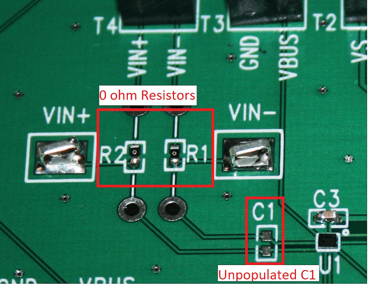
GUID-03576FEA-0787-478A-8CEA-ADDA2F54A60C-low.gifFigure 3-5 Typical Filter Setup