SBOU273A February 2022 – November 2022 INA851
7.2 PCB Layout
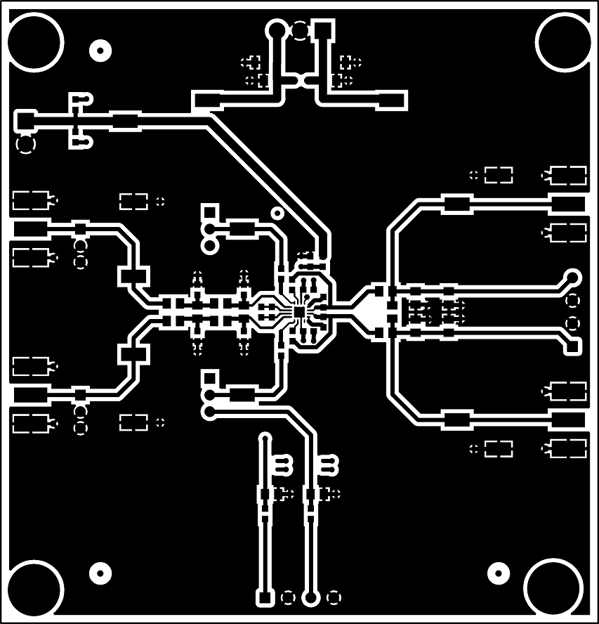
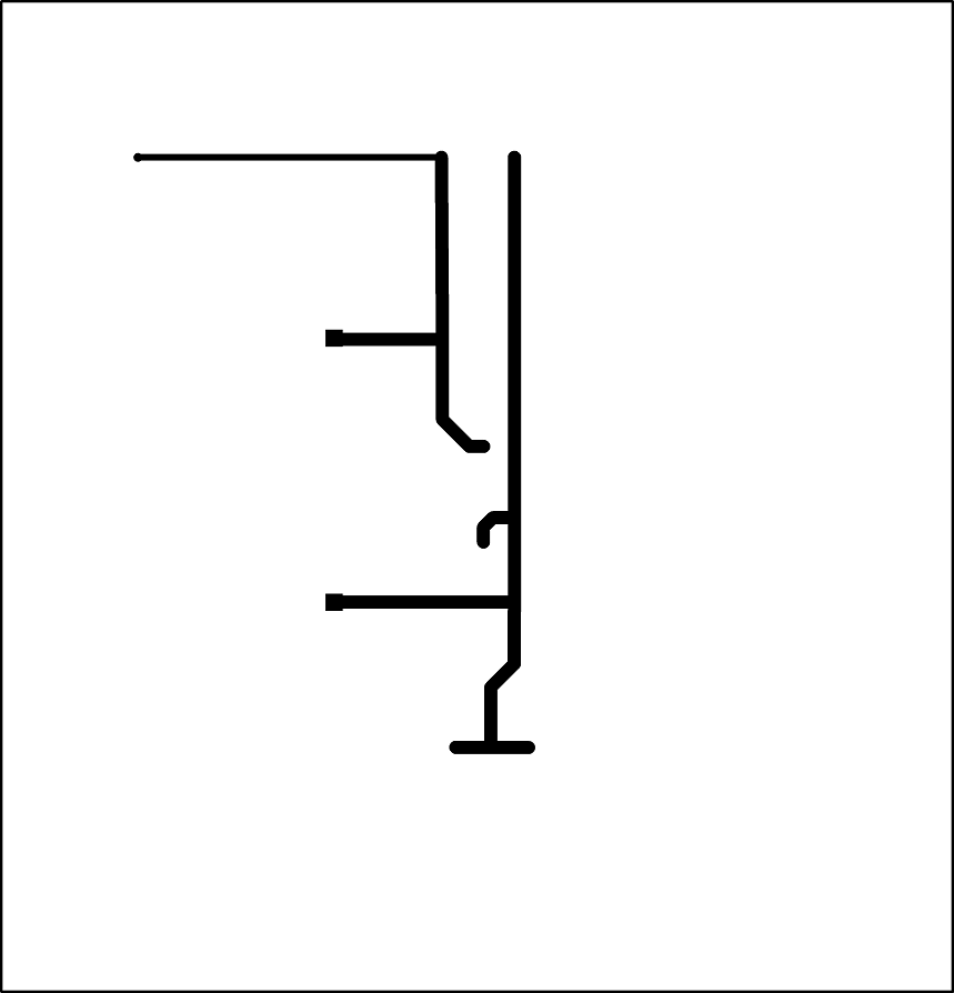
The INA851EVM is a four-layer PCB design. Figure 7-2 to Figure 7-6 show the PCB layer illustrations. The top layer consists of all signal path traces, and is poured with a solid ground plane. A symmetrical board layout is used at the differential inputs and outputs to keep good performance matching and improve common-mode noise rejection. Route traces as symmetrically as possible for both positive and negative pathways. Gain resistors RG1 and RG2 are placed on the top layer in close proximity to the device to reduce parasitic capacitance. Capacitor C5 is placed in close proximity to VOCM to avoid injecting common-mode noise. Decoupling capacitors C6, and C17 are positioned on the top layer as close as possible to the power-supply pins of the device. The second internal layer is a dedicated solid GND plane. Independent vias are placed at the ground connection of every component to provide a low-impedance path to ground. The third internal layer and bottom layer route the power supplies and the VCLAMP+ and VCLAMP– connections.
 Figure 7-2 Top Overlay PCB Layout
 Figure 7-3 Top Layer PCB Layout
 Figure 7-4 Ground Layer PCB Layout
 Figure 7-5 Power Layer PCB Layout
 Figure 7-6 Bottom Layer PCB Layout