SBOU293E November   2022  – August 2024


  1.   1
  2.   Description
  3.   Features
  4.   4
  5. 1Evaluation Module Overview
    1. 1.1 Introduction
    2. 1.2 OPTEVM Kit Contents
    3. 1.3 Device Information
  6. 2Hardware
    1. 2.1 OPTEVM Hardware Overview
  7. 3Software
    1. 3.1 OPTEVM Software
      1. 3.1.1 Hardware Requirements
      2. 3.1.2 Software Installation
      3. 3.1.3 Typical OPTEVM Hardware Setup
      4. 3.1.4 Launching the OPT300x/4xxxEVM Software
      5. 3.1.5 OPTEVM Software Operation
        1. 3.1.5.1 Getting Started
        2. 3.1.5.2 Feature Descriptions
          1. 3.1.5.2.1 Lux Plot
          2. 3.1.5.2.2 Mean, Std, and the Blue Slider
      6. 3.1.6 Controls
        1. 3.1.6.1 Capture Controls
          1. 3.1.6.1.1 Start Capture and Stop Capture
          2. 3.1.6.1.2 Display Sample Count
          3. 3.1.6.1.3 Save to File
        2. 3.1.6.2 Device Controls
          1. 3.1.6.2.1 Mode Select
          2. 3.1.6.2.2 Conversion Time
        3. 3.1.6.3 Operation Controls
          1. 3.1.6.3.1 Operation Select
          2. 3.1.6.3.2 Measurement/Capture Trigger
          3. 3.1.6.3.3 Oneshot Time (μs)
      7. 3.1.7 OPTxxxDTSEVM Variants
        1. 3.1.7.1 OPT4048DTSEVM
          1. 3.1.7.1.1 OPT4048DTSEVM CIE XY Window
          2. 3.1.7.1.2 OPT4048DTSEVM Lux Live Window
          3. 3.1.7.1.3 OPT4048DTSEVM Channel Live Window
        2. 3.1.7.2 OPT4060DTSEVM
          1. 3.1.7.2.1 OPT4060DTSEVM Channel Live Window
          2. 3.1.7.2.2 OPT4060DTSEVM Lux Live Window
      8. 3.1.8 Scripts Window
        1. 3.1.8.1 Additional Features of the Scripts Window
          1. 3.1.8.1.1 Hidden IDE Window
          2. 3.1.8.1.2 devInit.py
          3. 3.1.8.1.3 04-launchGUI.py
        2. 3.1.8.2 Overview of Device Registers: OPT4xxx Devices
  8. 4Hardware Design Files
    1. 4.1 Coupon Board
      1. 4.1.1 Schematic
      2. 4.1.2 PCB Layout DTS Package
      3. 4.1.3 Bill of Materials (BOM)
    2. 4.2 Motherboard
      1. 4.2.1 Schematic
      2. 4.2.2 PCB Layout
      3. 4.2.3 Bill of Materials
  9. 5Additional Information
    1. 5.1 Trademarks
    2. 5.2 Troubleshooting
      1. 5.2.1 Microsoft Windows 7 Manual Driver Installation
  10. 6Related Documentation from Texas Instruments
  11. 7Revision History

Overview of Device Registers: OPT4xxx Devices

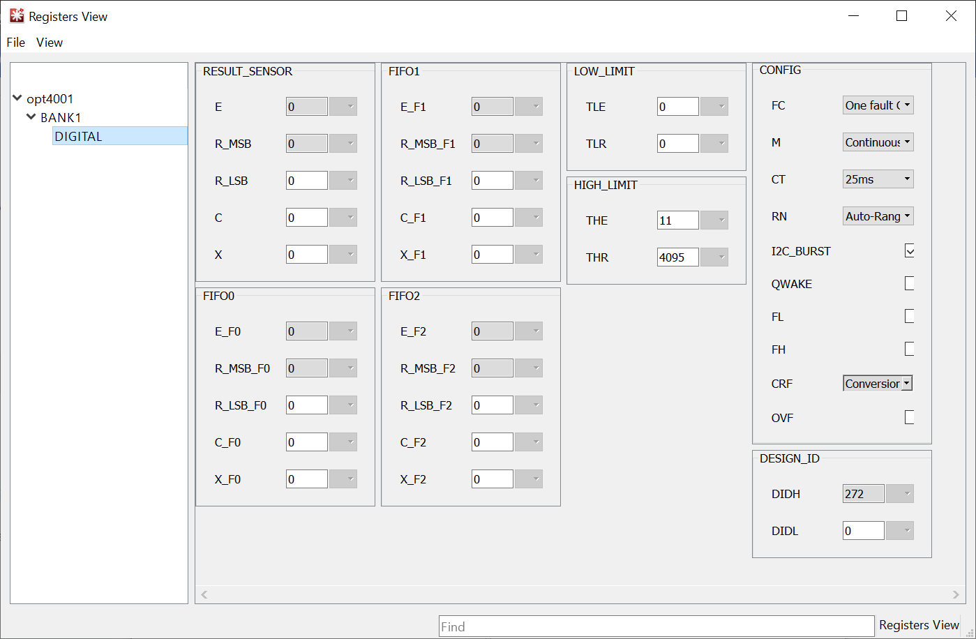
OPT3005DTSEVM OPT3005EVM OPT4001DTSEVM OPT4048DTSEVM Registers View Example for
                    OPT4xxx Devices Figure 3-21 Registers View Example for OPT4xxx Devices

Registers E, R_MSB, R_LSB, C and X are the result registers for single channel devices with registers 0x02 through 0x07 as FIFO registers. The result register provides the output data from the device as an exponent and mantissa value indicated as e and r in the register view. The mantissa is split between registers 0x00 and 0x01 as R_MSB and R_LSB. A sample counter (C) and CRC check bits (X) are also contained in register 0x01.

For color sensors, registers 0x00 through 0x07 are the result registers for each channel.

Registers 0x0A, 0x0B, and 0x0C are the configuration registers and provide feedback about the state of the device; the bit names and full descriptions are shown in the device data sheet. Each of the read-only status bits are grayed out and cannot be changed. Registers x08 and x09 allow low and high limits, respectively, to be set. These registers are used in certain interrupt reporting modes. The Design_ID is contained in register 0x11.