SBOU317 September 2024
3.2 Board Layout
The board layers, in top to bottom order, are illustrated in Figure 3-2 through Figure 3-5.
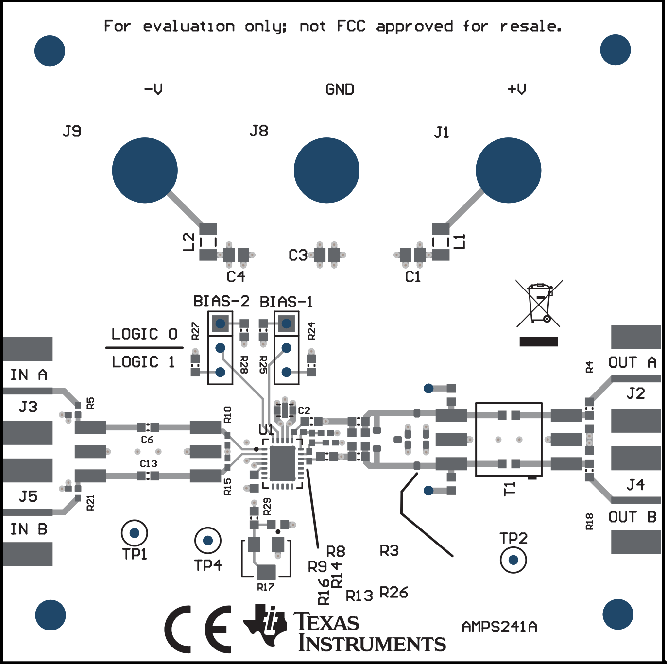 Figure 3-2 Top Layer
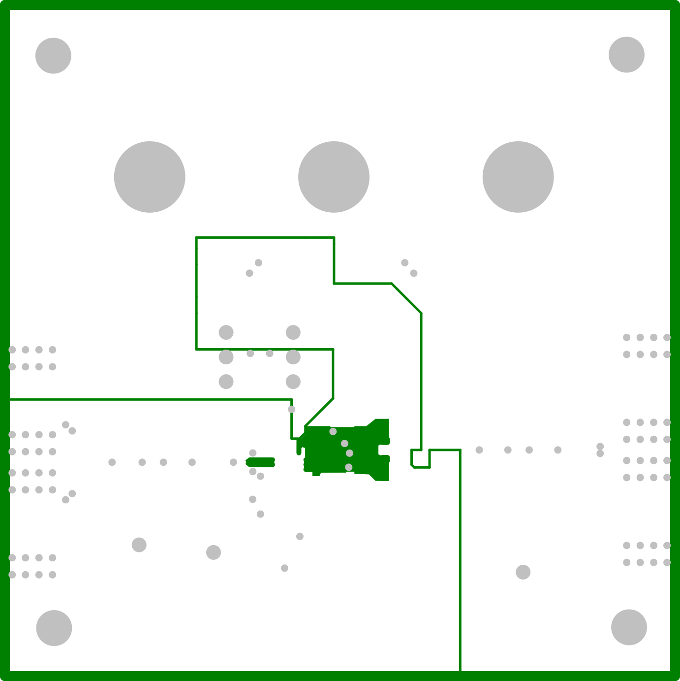 Figure 3-4 Power Layer
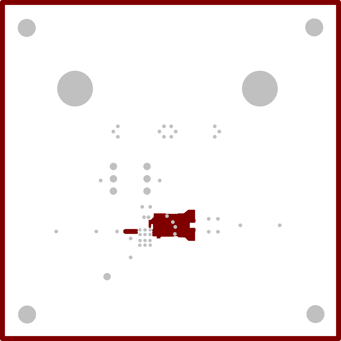 Figure 3-3 Ground Layer
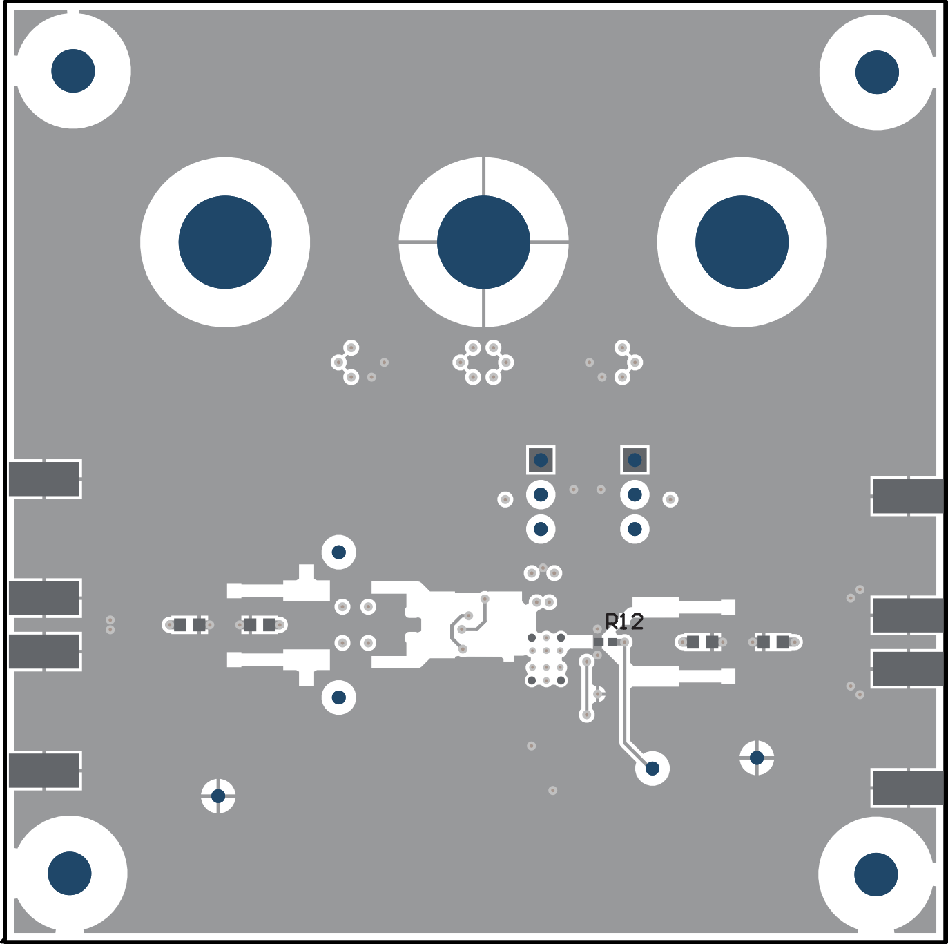 Figure 3-5 Bottom Layer
SBOU317 September 2024
The board layers, in top to bottom order, are illustrated in Figure 3-2 through Figure 3-5.
 Figure 3-2 Top Layer
 Figure 3-4 Power Layer
 Figure 3-3 Ground Layer
 Figure 3-5 Bottom Layer