SBVU080 September 2023
- 1
- Description
- Get Started
- Features
- Applications
- 6
- 1Evaluation Module Overview
- 2Hardware
- 3Hardware Design Files
- 4Additional Information
2.6 TRKRLDOEVM-119 Operation and Component Selection
The TRKRLDOEVM-119 evaluation module contains a SOT-23 footprint that also fits an SOIC-8 package, and pads for input and output capacitors. The prepopulated capacitors are sized to verify the minimum capacitance requirements are maintained under all normal operating conditions. Optional pads are available to test the LDO with additional setpoint options, as well as input and output capacitors beyond what is already installed on the EVM.
Setpoint resistors are prepopulated on the TRKRLDOEVM-119 to configure the TPS7B84-Q1 LDO with an output voltage of 3.3 V, 5 V, or 8 V. With a shunt placed across the pins of jumper J12, the output of the TPS7B84-Q1 supplies the ADJ/EN pin of the populated tracker LDO. If a different voltage than the TPS7B84-Q1 output is desired to drive the ADJ/EN pin, remove the shunt from jumper J12 and use a combination of J5, R2, R5, and C11 to configure the ADJ/EN pin to be a function of the input voltage. Alternatively, TP1 and TP2 can be used to directly drive ADJ/EN with an external voltage source.
The TPS7B84-Q1 LDO can be enabled or disabled by using the J13 3-pin header:
- Place a 2-pin shunt across the header to tie VIN to EN to enable the device
- Place a 2-pin shunt across the header to tie GND to EN to disable the device
Alternatively, by connecting an external function generator to TP3 (EN) and TP2 (GND), the user can enable or disable the TPS7B84-Q1 LDO after VIN is applied.
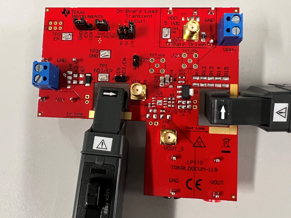
If desired, a current probe can be inserted in the EVM as illustrated in Figure 3-1 to measure the input and output current. The slots were sized to fit most current probes, such as the LeCroy™ AP015 or CP031 current probes.
The board layout is designed such that the Iin current probe slot does not detect any current that goes to the TPS7B84-Q1 circuit or the peripherals during start up or during any other operational mode. Thus, the Iin current probe slot can be used to isolate and accurately measure current into the tracker LDO device.
 Figure 2-1 TRKRLDOEVM-119 With Current
Probes Attached
Figure 2-1 TRKRLDOEVM-119 With Current
Probes AttachedThe user has two options for providing a DC load on the output of the tracker LDO. J7 can be used to place a DC load that flows through the current sense path on the output of the LDO. Alternatively, the J4 (VOUT) and J11 (GND) banana connectors can be used for external measurements and loading; however, the IOUT loop does not sense current flowing through these connectors. In cases where very fast transient tests are performed, ringing can occur on VIN or VOUT as a result of the PCB parasitic inductance. Placing a strip of wire on the exposed copper in the current path can reduce this ringing. 10 AWG wire can be used as needed. If ringing persists, install damping networks by adding a series resistor and capacitor in parallel with VIN. Locations where damping can be installed include C2 and R4, and C16 and R22.
Optional kelvin sense points are provided using the SMA connectors J1 (VIN) and J2 (VOUT).