SBVU085 December 2024
2.1.4.1 TPS7N53 LDO Operation
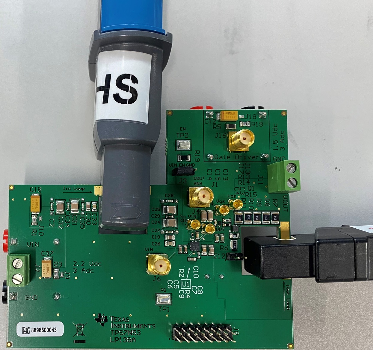
The TPS7N53 evaluation module contains a single TPS7N53 LDO with input, NR, SS, and output capacitors installed, as well as PG and REF resistors installed. These components provide an implementation example, as illustrated by TPS7N53EVM-138 With Current Probes Attached.
The TPS7N53 EVM is assembled for an output voltage of 0.75V. For other voltage options, resistor R4 can be modified as necessary. See the Adjustable Operation section in the TPS7N53 data sheet for guidance on selecting R4 for alternate values of VOUT.
The TPS7N53 LDO can be enabled or disabled by using the J3 jumper connection:
- Tie the center pin of the jumper to a voltage source greater than 0.68V and no greater than 6.0V to enable the device
- Tie the center pin of the jumper to a voltage source less than 0.64V to disable the device
If desired, then current probes can be inserted in the EVM as shown in Figure 2-2 to measure the input and output current. The slots were sized to fit most current probes, such as the LeCroy™ AP015 or CP031 current probes. The input and output current of the TPS7N53 LDO can be measured directly using the current probes.
 Figure 2-2 TPS7N53EVM With Current Probes
Attached
Figure 2-2 TPS7N53EVM With Current Probes
AttachedJ11 can be used to place a DC load that flows through the current sense path on the output of the LDO. In cases where very fast transient tests are performed, ringing can occur on VIN or VOUT as a result of the PCB parasitic inductance. Placing a strip of wire on the exposed copper in the current path can reduce this ringing. 10 AWG wire can be used as needed. If ringing persists, then install damping networks by adding a series resistor and capacitor in parallel with VIN. Locations where damping can be installed include C20 and R24, C18 and R1, and C37 and R3.
Optional kelvin sense points are provided using the SMA connectors J6 (VIN) and J4 (VOUT) and MMCX connectors J5 (VIN) and J1 (VOUT).
Optional Load Transient Circuit Operation
The TPS7N53 evaluation module contains an optional high-performance load transient circuit to allow efficient testing of the load transient performance of the TPS7N53 LDO. To use the optional load transient circuit, install the correct components in accordance with the application. Modify the input and output capacitance connected to the TPS7N53 LDO to match the expected operating conditions. Determine the desired peak current to test, and modify the parallel resistor combination of R7, R8, R9, R10, and R11 as shown:
The slew rate of the load step can be adjusted by C11, R12, R13, and R14.
After the load transient circuit is modified as needed, connect a power supply to banana connectors J15 (VDD) and J19 (GND) with a 5V DC supply and a 500mA DC current limit. Use a pulse-duration limit of 1ms to prevent excessive heating of the pulsed resistors (R7, R8, R9, R10, and R11). Configure a function generator for the 50Ω output, in a 0V DC to 5V DC square pulse. If necessary, burst mode can be configured in the function generator for repetitive, low duty cycle, load transient testing.