SBVU085 December   2024


  1.   1
  2.   Description
  3.   Features
  4.   Applications
  5.   5
  6. 1Evaluation Module Overview
    1. 1.1 Introduction
    2. 1.2 Kit Contents
    3. 1.3 Specification
    4. 1.4 Device Information
  7. 2Hardware
    1. 2.1 Power Requirements
      1. 2.1.1 EVM Connections
      2. 2.1.2 Test Equipment
      3. 2.1.3 Recommended Test Setup
        1. 2.1.3.1 Input Connections
        2. 2.1.3.2 Output Connections
      4. 2.1.4 Test Procedure
        1. 2.1.4.1 TPS7N53 LDO Operation
  8. 3Implementation Results
    1. 3.1 Performance Data and Results
  9. 4Hardware Design Files
    1. 4.1 Schematics
    2. 4.2 PCB Layouts
    3. 4.3 Bill of Materials (BOM)
  10. 5Compliance Information
    1. 5.1 Compliance and Certifications
  11. 6Additional Information
    1. 6.1 Trademarks
  12. 7Related Documentation
    1. 7.1 Supplemental Content

Schematics

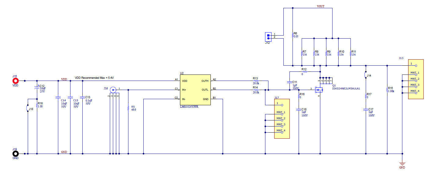
Figure 4-1 through Figure 4-3 show the EVM schematics.

Figure 4-1 TPS7N53EVM Schematic TPS7N53EVM-138
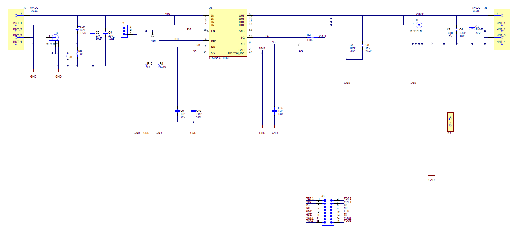
Figure 4-2 Input Capacitor Schematic TPS7N53EVM-138
Figure 4-3 Load Transient Schematic TPS7N53EVM-138