SBVU085 December   2024


  1.   1
  2.   Description
  3.   Features
  4.   Applications
  5.   5
  6. 1Evaluation Module Overview
    1. 1.1 Introduction
    2. 1.2 Kit Contents
    3. 1.3 Specification
    4. 1.4 Device Information
  7. 2Hardware
    1. 2.1 Power Requirements
      1. 2.1.1 EVM Connections
      2. 2.1.2 Test Equipment
      3. 2.1.3 Recommended Test Setup
        1. 2.1.3.1 Input Connections
        2. 2.1.3.2 Output Connections
      4. 2.1.4 Test Procedure
        1. 2.1.4.1 TPS7N53 LDO Operation
  8. 3Implementation Results
    1. 3.1 Performance Data and Results
  9. 4Hardware Design Files
    1. 4.1 Schematics
    2. 4.2 PCB Layouts
    3. 4.3 Bill of Materials (BOM)
  10. 5Compliance Information
    1. 5.1 Compliance and Certifications
  11. 6Additional Information
    1. 6.1 Trademarks
  12. 7Related Documentation
    1. 7.1 Supplemental Content

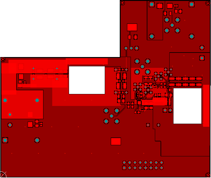
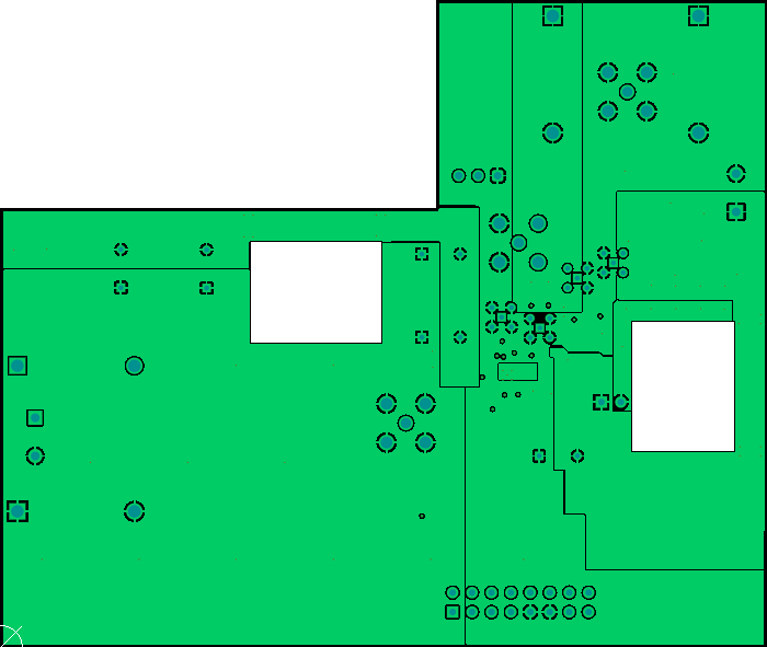
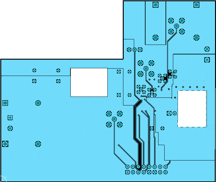
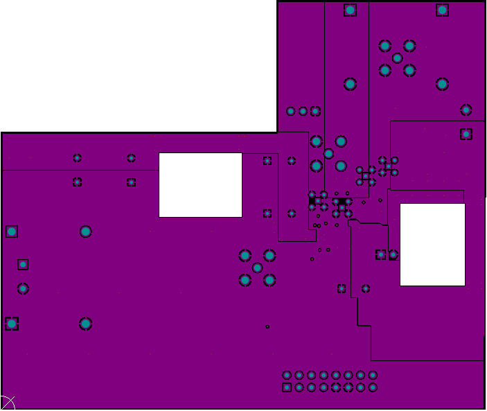
PCB Layouts

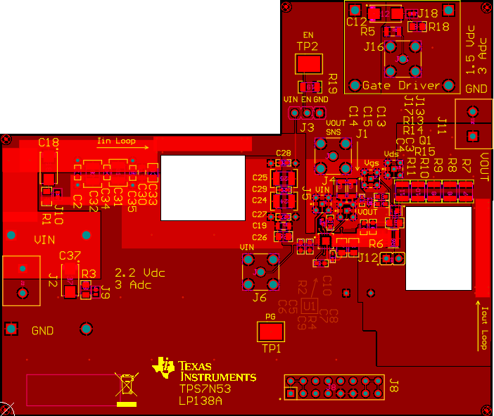
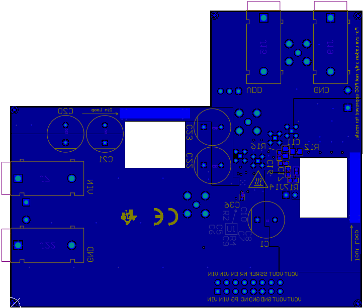
TPS7N53EVM-138 Top
                        Assembly Layer and SilkscreenFigure 4-4 Top Assembly Layer and Silkscreen
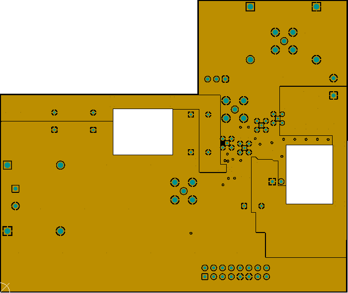
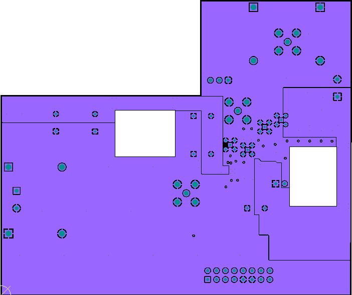
TPS7N53EVM-138 Layer
                        2Figure 4-6 Layer 2
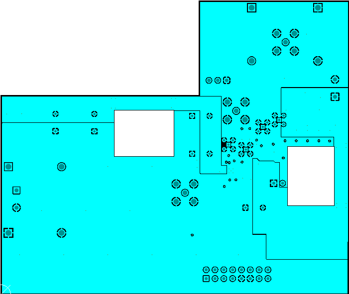
TPS7N53EVM-138 Layer
                        4Figure 4-8 Layer 4
TPS7N53EVM-138 Layer
                        6Figure 4-10 Layer 6
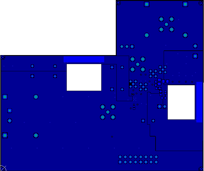
TPS7N53EVM-138 Bottom Layer RoutingFigure 4-12 Bottom Layer Routing
TPS7N53EVM-138 Top
                        Layer RoutingFigure 4-5 Top Layer Routing
TPS7N53EVM-138 Layer
                        3Figure 4-7 Layer 3
TPS7N53EVM-138 Layer
                        5Figure 4-9 Layer 5
TPS7N53EVM-138 Layer
                        7Figure 4-11 Layer 7
TPS7N53EVM-138 Bottom Assembly Layer and SilkscreenFigure 4-13 Bottom Assembly Layer and Silkscreen