SCDA036A May 2022 – June 2024 TMUX8212
- 1
- Abstract
- Trademarks
- 1 Size Requirement
- 2 Reliability Over Time
- 3 Power Consumption
- 4 Switching Speed and Hot Switching
- 5 Signal Isolation
- 6 Capacitance
- 7 On-Resistance and Flatness
- 8 Leakage Current
- 9 Integrated Protection
- 10Latch-up Immunity
- 11Galvanic Isolation
- 12Conclusion
- 13References
- 14Revision History
1 Size Requirement
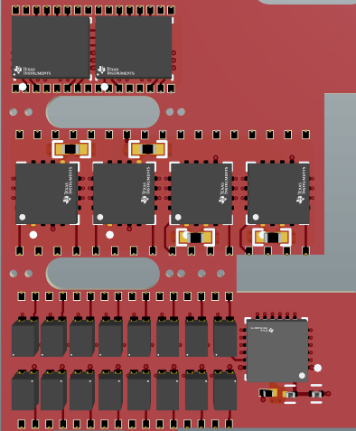
One of the largest benefits to an integrated multiplexer switching design is size. For example, in a 16-channel system, 16 SPST (1:1) mechanical relays would be needed, accounting for >450mm2 board area. This is before including any relay driver ICs. Compare this to a Photorelay design and the user can see that the size requirements reduce dramatically. But Photorelays can not be driven directly through GPIO and need an LED driver to control the state of each switch. This adds to the design size and increases the system complexity, as well as power requirements. TI’s Multiplexer design such as the TMUX821x and TMUX7612 do not require any additional ICs. Each individual switch can be controlled by standard digital pins with 1.8V Logic. As a result, TI’s switch design is even smaller than a comparable Photorelay design.
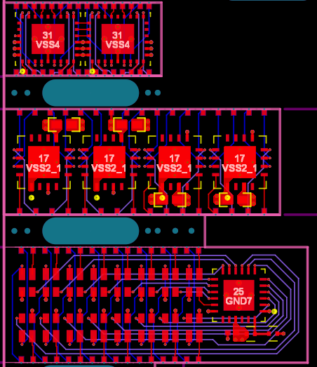
 Figure 1-1 16 Channel, 50V design
Size Comparison (drawn to scale)
  Figure 1-2 TMUXS7614D top,
TMUX7612/TMUX8212 middle, Photorelay Bottom
 As design size becomes a larger concern, routing and layout become a major consideration. The table below compares the actual design size of these three options with routing. You can see while the package density of the TMUX7612 and Photorelay are similar, when routing and layout is considered the space savings is more significant. And the TMUXS7614D saves significantly more area on top of this by integrating the passive components and optimizing the pinout.
TMUXS7614D |
TMUX7612 TMUX8212 |
Photorelay | |
|---|---|---|---|
| Total Package Area | 2.5mm2/ch | 4.0mm2/ch | 4.2mm2/ch |
| Total PCB Area | 3.18mm2/ch | 9.13mm2/ch | 11.22mm2/ch |
| Area Savings | 129mm2 (70% reduction) | 33.5mm2 (20% reduction) | - |