SFFS622 april 2023 OPA333-Q1
4 Pin Failure Mode Analysis (Pin FMA)
This section provides a Failure Mode Analysis (FMA) for the pins of the OPA333-Q1. The failure modes covered in this document include the typical pin-by-pin failure scenarios:
- Pin short-circuited to Ground (see Table 4-2)
- Pin open-circuited (see Table 4-3)
- Pin short-circuited to an adjacent pin (see Table 4-4)
- Pin short-circuited to supply (see Table 4-5)
Table 4-2 through Table 4-5 also indicate how these pin conditions can affect the device as per the failure effects classification in Table 4-1.
Table 4-1 TI Classification of Failure Effects
| Class | Failure Effects |
|---|---|
| A | Potential device damage that affects functionality |
| B | No device damage, but loss of functionality |
| C | No device damage, but performance degradation |
| D | No device damage, no impact to functionality or performance |
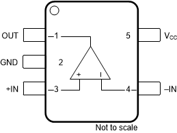
Figure 4-1 shows the OPA333-Q1 pin diagram. For a detailed description of the device pins, see the Pin Configuration and Functions section in the OPA333-Q1 data sheet.
 Figure 4-1 Pin Diagram
Following are the assumptions of use and the device configuration assumed for the pin FMA in this section:
- 'Short circuit to Power or VCC' means short to V+.
- 'Short circuit to GND or Ground' means short to V‒.
Table 4-2 Pin FMA for Device Pins Short-Circuited to Ground
| Pin Name | Pin No. | Description of Potential Failure Effect(s) | Failure Effect Class |
|---|---|---|---|
| OUT | 1 | Depending on the circuit configuration, the device is likely to be forced into a short-circuit condition with the OUT voltage ultimately forced to the GND voltage. Prolonged exposure to short-circuit conditions can result in long-term reliability issues. | A |
| +IN | 3 | Device common-mode is tied to the negative rail. Depending on the circuit configuration, the output likely does not respond due to the device in an invalid common-mode condition. | C |
| VCC | 4 | Op-amp supplies are shorted together, leaving the VCC pin at some voltage between the VCC and GND sources (depending on the source impedance). | A |
| ‒IN | 5 | The device does not receive negative feedback. Depending on the circuit configuration, the output most likely moves to the negative supply. | B |
Table 4-3 Pin FMA for Device Pins Open-Circuited
| Pin Name | Pin No. | Description of Potential Failure Effect(s) | Failure Effect Class |
|---|---|---|---|
| OUT | 1 | No negative feedback or ability for OUT to drive the application. | B |
| GND | 2 | Negative supply is left floating. The op amp ceases to function due to inability to source or sink current to the device. | B |
| +IN | 3 | Device common-mode is disconnected. The op amp is not provided with common-mode bias, and the device output likely ends up at the positive or negative rail. The +IN pin voltage likely ends up at the positive or negative rail due to leakage on the ESD diodes. | B |
| VCC | 4 | Positive supply is left floating. The op amp ceases to function due to inability to source or sink current to the device. | A |
| ‒IN | 5 | Inverting pin of the op amp is left floating. Negative feedback is not provided to the device, likely resulting in the device output moving between the positive and negative rails. The ‒IN pin voltage likely ends up at the positive or negative rail due to leakage on the ESD diodes. | B |
Table 4-4 Pin FMA for Device Pins Short-Circuited to Adjacent Pin
| Pin Name | Pin No. | Shorted to | Description of Potential Failure Effect(s) | Failure Effect Class |
|---|---|---|---|---|
| OUT | 1 | 2 | Depending on the circuit configuration, the device is likely to be forced into a short-circuit condition with the OUT voltage ultimately forced to the GND voltage. Prolonged exposure to short-circuit conditions can result in long-term reliability issues. | A |
| GND | 2 | 3 | Device common-mode is tied to the negative rail. Depending on the circuit configuration, the output likely does not respond due to the device in an invalid common-mode condition. | C |
| +IN | 3 | 4 | Depending on the circuit configuration, the application is likely not to function due to device common-mode voltage connected to +IN. | B |
| VCC | 4 | 5 | The device does not receive negative feedback. Depending on the noninverting input voltage and circuit configuration, the output most likely moves to the negative supply. | B |
| ‒IN | 5 | 1 | Depending on the circuit configuration, the circuit gain is reduced to unity gain, and the application might not function as intended. | B |
Table 4-5 Pin FMA for Device Pins Short-Circuited to supply
| Pin Name | Pin No. | Description of Potential Failure Effect(s) | Failure Effect Class |
|---|---|---|---|
| OUT | 1 | Depending on the circuit configuration, the device is likely to be forced into a short-circuit condition with the OUT voltage ultimately forced to the VCC voltage. Prolonged exposure to short-circuit conditions can result in long-term reliability issues. | A |
| GND | 2 | Op-amp supplies are shorted together, leaving the GND pin at some voltage between the GND and VCC sources (depending on the source impedance). | A |
| +IN | 3 | Depending on the circuit configuration, the application is likely not to function due to device common-mode voltage connected to +IN. | B |
| ‒IN | 5 | The device does not receive negative feedback. Depending on the noninverting input voltage and circuit configuration, the output most likely moves to the negative supply. | B |