SFFS759 February 2024 CD4051B-Q1
1 Overview
This document contains information for the CD4051B-Q1 (TSSOP package) to aid in a functional safety system design. Information provided are:
- Functional safety failure in time (FIT) rates of the semiconductor component estimated by the application of industry reliability standards
- Component failure modes and their distribution (FMD) based on the primary function of the device
- Pin failure mode analysis (pin FMA)
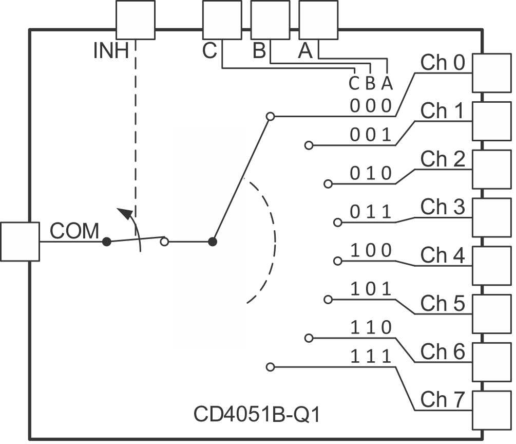
Figure 1-1 shows the device functional block diagram for reference.
 Figure 1-1 Functional Block
Diagram
Figure 1-1 Functional Block
DiagramThe CD4051B-Q1 was developed using a quality-managed development process, but was not developed in accordance with the IEC 61508 or ISO 26262 standards.