SFFS809 September 2024 TLV710-Q1
4 Pin Failure Mode Analysis (Pin FMA)
This section provides a failure mode analysis (FMA) for the pins of the TLV710-Q1. The failure modes covered in this document include the typical pin-by-pin failure scenarios:
- Pin short-circuited to ground (see Table 4-2)
- Pin open-circuited (see Table 4-3)
- Pin short-circuited to an adjacent pin (see Table 4-4)
- Pin short-circuited to VIN (see Table 4-5)
Table 4-2 through Table 4-5 also indicate how these pin conditions can affect the device as per the failure effects classification in Table 4-1.
| Class | Failure Effects |
|---|---|
| A | Potential device damage that affects functionality. |
| B | No device damage, but loss of functionality. |
| C | No device damage, but performance degradation. |
| D | No device damage, no impact to functionality or performance. |
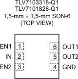
Figure 4-1 shows the TLV710-Q1 pin diagram. For a detailed description of the device pins, see the Pin Configuration and Functions section in the TLV710-Q1 data sheet.
 Figure 4-1 Pin Diagram
Following are the assumptions of use and the device configuration assumed for the pin FMA in this section:
- Device contains DSE pin configuration. Device operates at free-air temperatures between -40°C and 125°C.
- Device operates at an input voltage less than 5.5V and more than 2V.
- Device operates according to all recommended operating conditions and does not exceed the absolute maximum ratings.
| Pin Name | Pin No. | Description of Potential Failure Effects | Failure Effect Class |
|---|---|---|---|
| EN1 | 1 | LDO 1 is always off due to EN being grounded. | B |
| IN | 2 | Output voltage is at or near ground. | B |
| EN2 | 3 | LDO 2 is always off due to EN being grounded. | B |
| GND | 4 | No effect. Normal operation. | D |
| OUT2 | 5 | Output voltage 2 is at or near ground. Device is in current limit. The device can cycle in and out of thermal shutdown depending on power dissipation. | B |
| OUT1 | 6 | Output voltage 1 is at or near ground. Device is in current limit. The device can cycle in and out of thermal shutdown depending on power dissipation. | B |
| Pin Name | Pin No. | Description of Potential Failure Effects | Failure Effect Class |
|---|---|---|---|
| EN1 | 1 | LDO is in unknown state. | B |
| IN | 2 | No input to LDO. Output is at or near ground. | B |
| EN2 | 3 | LDO is in unknown state. | B |
| GND | 4 | There is no current loop for internal biasing; device cannot operate. | B |
| OUT2 | 5 | Device 2 output is unregulated and the load is not powered. | B |
| OUT1 | 6 | Device 1 output is unregulated and the load is not powered. | B |
| Pin Name | Pin No. | Shorted to | Description of Potential Failure Effects | Failure Effect Class |
|---|---|---|---|---|
| EN1 | 1 | IN | If EN is positive voltage above the IN absolute maximum rating, IN can be damaged. | A |
| IN | 2 | EN2 | If EN is positive voltage above the IN absolute maximum rating, IN can be damaged. | A |
| GND | 4 | OUT2 | Output voltage is at or near ground. Device is in current limit. The device can cycle in and out of thermal shutdown depending on power dissipation. | B |
| OUT2 | 5 | OUT1 | Output voltage is driven to unknown voltage. High current drive between pins is possible leading to potential thermal shutdown. | A |
| Pin Name | Pin No. | Description of Potential Failure Effects | Failure Effect Class |
|---|---|---|---|
| EN1 | 1 | If EN is positive voltage above the IN absolute maximum rating, IN can be damaged. | A |
| IN | 2 | No effect. Normal operation. | D |
| EN2 | 3 | If EN is positive voltage above the IN absolute maximum rating, IN can be damaged. | A |
| GND | 4 | Output voltage is at or near ground. | B |
| OUT2 | 5 | Regulation for LDO 2 is not possible. The output voltage equals input voltage. | B |
| OUT1 | 6 | Regulation for LDO 1 is not possible. The output voltage equals input voltage. | B |