SLAA828B March 2018 – August 2021 MSP430FR2000 , MSP430FR2032 , MSP430FR2033 , MSP430FR2100 , MSP430FR2110 , MSP430FR2111 , MSP430FR2310 , MSP430FR2311 , MSP430FR2422 , MSP430FR2433 , MSP430FR2512 , MSP430FR2522 , MSP430FR2532 , MSP430FR2533 , MSP430FR2632 , MSP430FR2633 , MSP430FR4131 , MSP430FR4132 , MSP430FR4133
1 Introduction
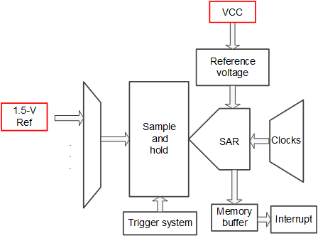
The 10-bit ADC module of MSP430FR2xx and MSP430FR4xx products is shown in Figure 1-1. The ADC acquisition channel can directly sample the internal voltage reference (typically 1.5 V, see the data sheet for details), and the ADC reference voltage can be configured as the supply voltage. The ADC input channel detailed information can be found in the "ADC Channel Connections" table in the device data sheet. Configure the ADCINCHx bits in the ADCMCTL0 register as defined in the table to use a 1.5-V reference as the input voltage. The reference voltage for the ADC is configured as 000b for the ADCSREFx bits.
 Figure 1-1 On-Chip
Measurement of Battery Voltage Diagram
Figure 1-1 On-Chip
Measurement of Battery Voltage DiagramEquation 1 shows how to calculate the 10-bit ADC conversion results.

where
- NADC = ADC conversion results
- Vin = Channel acquisition voltage
- VR+ = Reference voltage positive
- VR- = Reference voltage negative
Set Vin to the on-chip 1.5-V reference source, set VR+ to VCC, and set VR- to VSS. Equation 2 shows the formula to calculate the supply voltage.

Compared with the traditional solutions, on-chip ADC detection solution has the following advantages:
- Power consumption: the traditional method requires a peripheral voltage divider circuit, while the voltage divider circuit gives the system extra power consumption.
- Cost: the use of on-chip measurement method can save four resistors and a transistor; in addition, it can save 1 to 2 I/O resources.
- Volume: there is no peripheral voltage divider circuit that can reduce the size of the PCB for users.