SLAA870 February 2019 AFE7422 , AFE7444
-
Evaluating the frequency hopping capability of the AFE74xx
- Trademarks
- 1 Introduction
- 2 Phase Coherency vs Phase Continuity
- 3 AFE74xx Architecture
- 4 Frequency Hopping Methods
- 5 NCO Frequency Resolution Versus Hop Time
- 6 Fast Frequency Hopping With the Load and Switch
- 7 Register Addresses
- 8 References
4.2.2 RX NCO Hopping Using the GPIO Pins
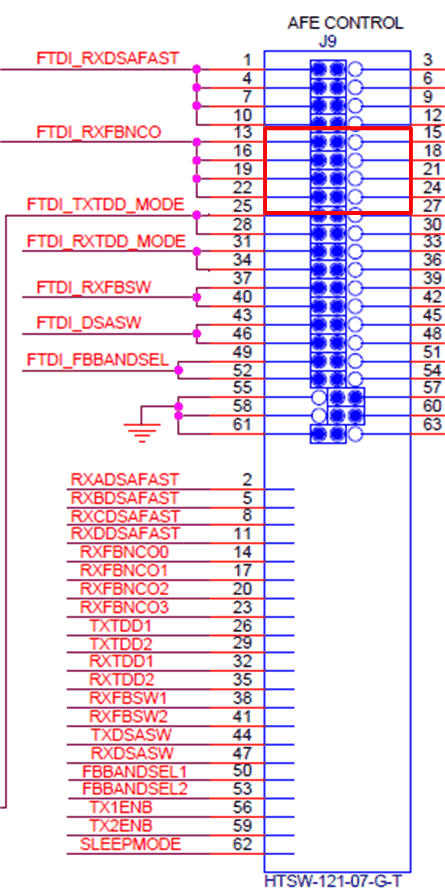
If a receiver application requires three NCO for frequency hopping, the AFE74xx supports seamless hopping using the GPIO pins in real time. The advantage of this method is that no SPI writes are required to change NCOs, thus greatly reducing hop time. There are two GPIO pins per two receivers: RXFBNCO0 and RXFBNCO1 for RX channels A and B, respectively; and RXFBNCO2 and RXFBNCO3 for RX channels C and D, respectively. Figure 22 shows where GPIO pins RXFBNCO0 to RXFBNCO3 are located.
 Figure 22. AFE74xx Pinbank J9 Containing RX NCO GPIO Pins
 Table 2 shows the relationship between enabled GPIO pins to selected NCO.
Table 2. Relationship Between Enabled GPIO Pins to Selected NCO
| GPIO Pin | NCO ID | |
|---|---|---|
| RXFBNCO-1/3 | RXFBNCO-0/2 | |
| 0 | 0 | NCO_0 |
| 0 | 1 | NCO_1 |
| 1 | 0 | NCO_2 |
| 1 | 1 | Not applicable |