SLAA988A December 2020 – January 2022 TAS2563
1.3 DREG
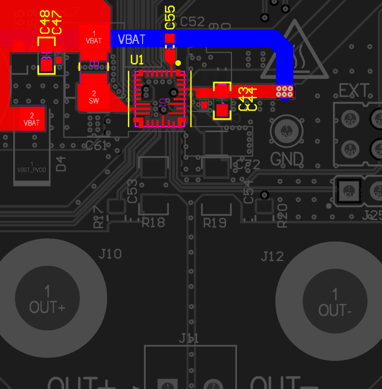
DREG is the digital core voltage regulator output. This pin must be bypassed to GND with a 1-µF capacitor and it must not be connected to an external load. TI recommends ensuring that both decoupling capacitor ends see as low inductance as possible between this DREG pin and GND. Multiple vias are suggested to reduce the inductance. See the Decoupling Capacitors section for details.
 Figure 1-5 DREG Connection