SLAAED9 November   2023 TAA5412-Q1 , TAC5311-Q1 , TAC5312-Q1 , TAC5411-Q1 , TAC5412-Q1


  1.   1
  2.   Abstract
  3.   Trademarks
  4. Introduction
  5. Diagnostic Monitoring Architecture
  6. Monitored Faults
    1. 3.1 Microphone Faults
      1. 3.1.1 Inputs Shorted to Ground
      2. 3.1.2 Inputs Shorted to MICBIAS
      3. 3.1.3 Input Open Circuit
      4. 3.1.4 Input Pins Shorted Together
      5. 3.1.5 Input Overvoltage Detection
      6. 3.1.6 Inputs Shorted to VBAT
    2. 3.2 Line Out Faults
      1. 3.2.1 Output Overcurrent
      2. 3.2.2 Virtual Ground
    3. 3.3 Other Faults
      1. 3.3.1 MICBIAS Overvoltage
        1. 3.3.1.1 DIAG_CFG11 Register (page = 0x01, address = 0x51) [Reset = 0x40]
      2. 3.3.2 MICBIAS Overcurrent
      3. 3.3.3 MICBIAS Load Current
        1. 3.3.3.1 DIAG_CFG6 Register (page = 0x01, address = 0x4C) [Reset = 0xA2]
        2. 3.3.3.2 DIAG_CFG7 Register
      4. 3.3.4 Overtemperature Fault
      5. 3.3.5 Supply Back Pumping
  7. Enabling Diagnostics and Programming Thresholds
    1. 4.1 DIAG_CFG0 Register (page = 0x01, Address = 0x46) [Reset = 0x00]
    2. 4.2 DIAG_CFG1 Register (page = 0x01, Address = 0x47) [Reset = 0x37]
    3. 4.3 DIAG_CFG2 Register (page = 0x01, Address = 0x48) [Reset = 0x87]
  8. Fault Diagnostic Setup Procedure
  9. Fault Reporting
    1. 6.1 Live Registers
      1. 6.1.1 CHx_LIVE Register (page = 0x01, address = 0x3D) [Reset = 0b]
      2. 6.1.2 CH1_LIVE Register (page = 0x01, address = 0x3E) [Reset = 0h]
      3. 6.1.3 INT_LIVE0 Register (page = 0x01, address = 0x3C) [Reset = 00]
      4. 6.1.4 INT_LIVE1 Register (page = 0x00, address = 0x42) [reset = 0x00]
      5. 6.1.5 INT_LIVE2 Register (page = 0x00, address = 0x43) [reset = 0x00]
    2. 6.2 Latched Registers
      1. 6.2.1 Clearing Latched Registers
    3. 6.3 Fault Filtering and Response Time
      1. 6.3.1 Debounce
      2. 6.3.2 Scan Rate
        1. 6.3.2.1 DIAG_CFG4 Register (page = 0x01, address = 0x4A) [reset = 0xB8]
      3. 6.3.3 Moving Average
        1. 6.3.3.1 DIAG_CFG5 Register (page = 0x01, address = 0x4B) [reset = 0h]
  10. Responding to a Fault
    1. 7.1 INT_CFG Register (page = 0x00, address = 0x42) [reset = 0b]
      1. 7.1.1 DIAG_CFG10 Register (page = 0x01, address = 0x50) [Reset = 0x88]
    2. 7.2 Manual Recovery Sequence
    3. 7.3 Recommended Fault Register Read Sequence
  11. Using PurePath Console
    1. 8.1 Advanced Tab
    2. 8.2 Diagnostics Walk-through
      1. 8.2.1 Diagnostics Configuration
      2. 8.2.2 Debounce Configuration
      3. 8.2.3 Latched Fault Status
  12. Diagnostic Monitoring Registers
    1. 9.1 Voltage Measurements
    2. 9.2 MICBIAS Load Current
    3. 9.3 Internal Die Temperature
  13. 10Summary
  14. 11References

Input Pins Shorted Together

This fault triggers when the absolute value of the difference between the input pins falls under the programmed threshold. This fault is programmable from 0 V to 450 mV in steps of 30 mV. In a typical DC-coupled application, there is a differential DC offset between the input pins from the microphone. This fault can trigger inadvertently in the application if the DC differential is kept below the programmed threshold.
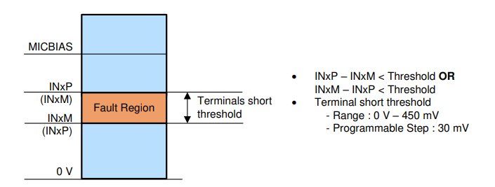
GUID-20230928-SS0I-XTGF-PK4H-5RPZ4JG2TPMQ-low.png Figure 3-4 Inputs Shorted Conditions